Signal Path Block Diagram
The following picture shows the block diagram of the signal path of the Variable Gain Board. The control circuitry, AGC detector and slow and fast feedback paths have all been left out in order to focus on the open loop behavior of the signal path.
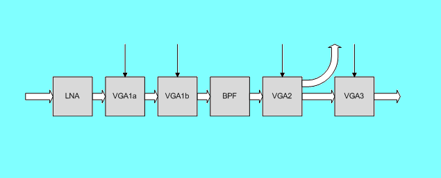
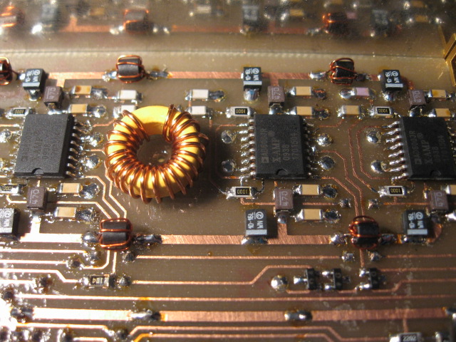
The signal path consists of 5 cascaded wideband amplifiers with only one band-pass filter centered at 9MHz. This single filter can also easily be scaled to allow for another IF frequency than 9MHz. There are 4 individual VGA blocks, preceded by a fixed gain LNA. VGA3 is also outside the AGC control loop and gets feed forward correction to achieve complete gain flattening. The detailed schematic of the signal path can be found on Sheet 1 and Sheet 2 in the Variable Gain Board documentation .pdf file. The following picture shows a close-up of the VGA1a, VGA1b, BPF and VGA2 section of the signal path from right to left. Note the inter-stage power supply decoupling measures on the PCB:
Which VGA?
Central in the detailed design of the signal path is the choice of the VGA IC (Variable Gain Amplifier). In the original W7AAZ design the AD600 is used. AD600 uses the X-AMP topology which gives a very accurate linear in dB gain control interface. X-AMP was originally designed by Barrie Gilbert of ADI (well-known also from the Gilbert cell mixers!). AD600 is one of the first IC's introduced with the X-AMP topology and quite a few other VGA's have come out since then. Because AD600 is still one of the most expensive VGA IC's from Analog Devices it seemed useful to have a good look at other potential candidates. This turned out to be not so straightforward! Although today there is a wide choice of VGA's with analog gain control interface, not that many do fit the bill for the Variable Gain Board application. Key parameters are:
-
Gain Control Range
-
Maximum Gain
-
Noise Figure
-
Dynamic Range
Many VGA's do either have too much gain or not enough gain. Most have an insufficient noise figure and / or have less dynamic range than AD600. It is important to realize that the X-AMP topology consists of a precision variable attenuator followed by a fixed gain amplifier. This means that excess gain can only be reduced via the gain control interface at the cost of an increased noise figure by the same amount. This leaves very few alternatives. The most promising alternative to AD600 is AD8367, which is 4 times less expensive. It has a 45dB gain control range with a maximum gain of +42.5dB, which is slightly too much for 3 stages and not enough for 2 stages.
AD8367 has been seriously taken into consideration, but it is less good than the older AD600 when it comes to strong signal handling. AD8367 conveniently uses a single +5V supply, while AD600 needs a +5V and a -5V dual supply. This is probably the reason why AD600 can work with a few volt input and output signal, while AD8367 is limited to 700mVpp input signal in 200Ω. For this reason AD600 has been chosen to serve on the Variable Gain Board, as any compromise to the so hard earned strong signal behavior of the frontend is out of the question. The Variable Gain Board must be capable to swallow 0dBm antenna signals the frontend is capable of, while producing only negligible extra in-channel distortion!
AD600
AD600 is good on paper, but how good is AD600 in reality? AD600 has a very good noise specification when examining the datasheet. Typically a 2dB noise figure is projected for maximum gain and 200Ω Rs source impedance. This seems too good to be true and real tests show that it is not reproducible on the bench. Measurements show that the NF of a single AD600 amplifier is about 10,5dB. This is a huge difference with the claimed NF in the datasheet. The datasheet also shows an ultra low noise configuration with 2x AD600 in parallel, which should give a 3dB improvement over a single AD600. This configuration has been tested and its NF is 7.5dB, so indeed 3dB better than the single AD600 configuration. The schematic copied from the datasheet is shown in the following picture:
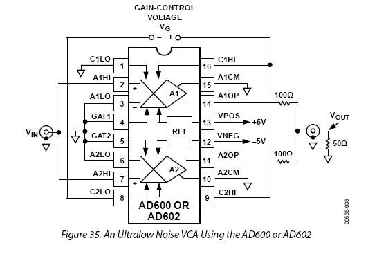
Unfortunately a NF of 7.5dB is not good enough for this application. The 7.5dB would degrade the cumulative noise figure of 8.8dB at the output of the Selectivity Board (SSB) to 10.3dB. Something below 3dB is needed in order to not further degrade the NF obtained by the frontend. Only just enough gain has been applied on the Selectivity Board to compensate for the insertion loss of the quality crystal filters, so the signal level at the input of the Variable Gain board is still critically low. Therefore without help AD600 cannot deliver the performance needed NF-wise and that is why the LNA block is found in front of the VGA's in the block diagram. We need about 10dB gain and a NF of 1.5dB in front of the AD600 to obtain the required performance.
The LNA block being used is a well-known circuit by now. Have a look at Sheet 1 in the documentation file and it can be recognized as the Quad J310 amplifier also deployed on the Selectivity Board. With a NF of around 1.3dB and gain of 12dB this LNA is perfect to raise the signal level such that the relatively poor NF of the AD600 X-AMP plays no significant role anymore. Also its +35dBm OIP3 is about sufficient for this application as the IMD will be < -60dBc for input signals < -7dBm. With this pre-amp, the NF of the Variable Gain Board is 2.15dB. The MDS measured in SSB bandwidth is -138dBm. Note that with a single AD600 amplifier instead of the parallel version, the cumulative NF is 3.0dB, almost 1dB worse. The cumulative noise figure seen at the board its input is not much degraded by the 2.15dB noise figure. The cumulative noise figure at its output is 9.04dB. That is only 0.25dB less than the 8.8dB at its input!
The following picture shows the quad J310 LNA at the far right. It uses the same "glue-on" heat sink technique as applied on the Selectivity Board to keep the MMBFJ310's a bit cooler.
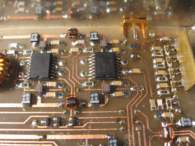
A single AD600 stage has a precise resistive input impedance laser trimmed within 2% accuracy at 100Ω. However the output stage of AD600 requires a minimum load resistance of a few hundred ohms in order to keep IMD low (-60dBc) and to be able to achieve the maximum peak output voltage. Therefore 200Ω output series resistors are found in the original W7AAZ circuit. This does introduce a significant -9.5dB drop in voltage gain between 2 cascaded stages. It would be better if we could work in a 50Ω system, because than only a -6dB voltage gain is encountered between 2 stages. This is where the 2x AD600 parallel low noise circuit comes back into focus!
We don't need so much the 1dB cumulative NF improvement with the parallel AD600's, but this circuit features 50Ω input and output impedance. Each individual AD600 actually sees 200Ω at its output, so distortion at high output levels is low. Another advantage of the parallel AD600 configuration is the more relaxed board layout. We now only have 40dB total gain in one IC instead of 80dB. A gain of 80dB, although doable in practice, is a bit much really. The input and output are very close together given the pinning of the IC and this may well be the reason that some have experienced stability problems with the original AD600 IF design, maybe amplified by using DIP IC's in sockets. The above pictures show a very straight forward PCB layout resulting in stability thanks to the dual VGA parallel amplifier approach.
Gain Distribution
Given the choice of LNA and AD600 parallel gain blocks, it is now possible to draw up an accurate gain distribution of the Variable Gain Board signal path. The following table shows the theoretical minimum and maximum gain per stage together with the accumulative gain:
| AD600 IF Gain distribution |
| Stage |
Gain (dB) |
Accumulative Gain (dB) |
| Minimum |
Maximum |
Minimum |
Maximum |
| LNA |
12.00 |
12.00 |
12.00 |
12.00 |
| 1st AD600 |
-1.07 |
41.07 |
10.93 |
53.07 |
| Output divider |
-6.02 |
-6.02 |
4.91 |
47.05 |
| 2nd AD600 |
-1.07 |
41.07 |
3.84 |
88.12 |
| Output divider |
-6.02 |
-6.02 |
-2.18 |
82.10 |
| BPF |
-2.00 |
-2.00 |
-4.18 |
80.10 |
| 3rd AD600 |
-1.07 |
41.07 |
-5.25 |
121.17 |
| Output divider |
-6.02 |
-6.02 |
-11.27 |
115.50 |
| AD602 |
5.33 |
10.00 |
-5.94 |
125.15 |
| Output divider |
-15.56 |
-15.56 |
-21.50 |
109.59 |
From input to output the gain is in between -21.5dB and +109.5dB. This is a total gain control range of 131dB. In total 126.4dB is provided by the three AD600's inside the feedback loop and 4.7dB is provided by the AD602 at the back by means of feed forward for gain flattening. In a practical closed-loop situation the gain control range is about 9.6dB less (121.4dB) as the first 300mV of the AGC voltage is used by the noise floor.
The following VNA picture shows the gain of the signal path when adjusted manually to minimum gain. Minimum gain can be obtained with I2C control of Vgain or by simply applying 3.9V on the Vext external analog gain control input. The VNA method is the preferred way to exactly center the BPF at 9MHz by (un)squeezing the windings of the toroid slightly.
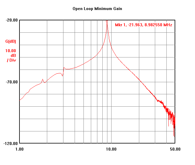
A gain of around -21dB is reached at 9MHz. The picture also shows the effect of the band-pass filter in between VGA1b and VGA2. More about the band-pass filter later. In order to accurately measure the gain and bandwidth at 9MHz the same situation is sweeped with a much smaller span as shown in the following graph:
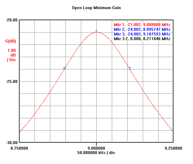
The minimum gain is -21.0dB which comes very close to the estimated -21.5dB from the gain distribution table. The -3dB bandwidth is 212 KHz.
Noise Filter
The purpose of the band-pass filter is to reduce the noise bandwidth of the amplifier. This is only needed for proper functioning of the AGC in closed-loop. Without this filter the much higher noise power of the wideband signal path will increase the AGC threshold to an unacceptable high value. In the previous picture it can be seen that the -3dB bandwidth of the filter is 212 KHz. This is about 80 times wider than the 2.7 KHz SSB bandwidth used in the original W7AAZ design! The original idea behind the narrow SSB filter inside the AGC loop is to have the AGC threshold start right at the noise floor of the receiver. This means that any signal at or above MDS will be level controlled by AGC action, including band noise. For the Variable Gain Board the idea is to follow a less radical AGC approach as I am not convinced that AGC action beginning at MDS is useful or will help to copy weak signals around the noise floor any better.
Another major reason to use a much wider noise bandwidth is to considerably improve AGC loop stability. The group-delay of a 3-pole Butterworth SSB quartz noise filter is approximately 300μs. This delay will introduce serious problems with stability when the loop is closed. Extensive SPICE simulation of closed-loop behavior showed that it is very difficult to get descent loop stability with such a narrow filter inside the loop. The 80 times wider bandwidth LC-filter used here improves loop stability greatly but causes the AGC threshold to be lifted by 10⋅log(80) = 19dB. This sets the AGC threshold at around S2, which is still acceptable.
The simplification of using a single LC filter after accumulating 82dB of wideband gain instead of filters in between all stages gave rise to a low frequency oscillation at around 20 KHz when the first prototype was first tested. One solution is to use a second filter between VGA1a and VGA1b, but a much easier fix is possible. By simply decreasing the DC blocking capacitors between the stages from 100n to 2.7n, the high-pass cut-off frequency goes up enough to stop this oscillation. Likewise C4 is used to provide some low-pass behavior above 9 MHz to improve stability also.
Another measure is necessary to ensure unconditional stability of the maximum 125dB gain on the Variable Gain Board. The two binocular transformers of the quad J310 amplifier must be mounted at the ground-plane side of the board, out of sight of the T50-6 toroid used in the LC noise filter. There is no oscillation with the 2 transformers mounted at the top side, but feedback is noticeable! The slope of the AGC voltage versus input signal strength is different for the first 80dB than for the last 40dB of the 120dB control range in the closed-loop case.
The signal path is unconditionally stable and reproducible thanks to the above measures together with the PCB layout and extensive power supply decoupling. This result is reproducible and does not require any fiddling with further shielding inside the box.
Gain Control Interface
The block diagram shows that VGA1a, VGA1b and VGA2 are all inside the AGC control loop and set the gain depending on signal strength when the loop is closed. However the loop gain is finite, so the output level will still increase slightly when the input signal goes from MDS to 0dBm. The increase at the end of the range at 0dBm is 4.7dB in this design. VGA3 is intended to precisely compensate for this affect and opposite gain control is applied in feed forward. VGA3 is implemented with AD602 which is identical to AD600 but maximum gain is 30dB with the same control range of 40db. This section is adjusted with fixed precision resistors to exactly provide the right amount of gain reduction in feed forward mode. There is no trim-pot adjustment made available for the gain flattening function. One likes the 100% gain flattening, or one dislikes it and then R84 is simply left out!
The other AD602 section in IC4 is setup to provide the right amount of fixed gain to feed the AGC detector: 16dB. Note that the GATE pin of that section can be controlled through I2C (VLOOP). When this pin is made logic high, the amplifier is disabled and this effectively causes the AGC loop to be opened allowing for a manual gain control mode.
AD600 has a differential gain control interface. The difference in voltage between the CxHI and CxLO pins determines the gain following the following approximate formula:
Gain (dB) = 32 * (V_CxHI - V_CxLO) + 20
This means that the maximum gain of approximately 40dB is achieved with +625mV and minimum gain of about 0dB is obtained with -625mV. Control voltage above +625mV and below -625mV does not change the gain. This is convenient and makes the gain control interface for multiple cascaded stages fairly simple. The AD600 datasheet mentions 2 different approaches to cascade multiple AD600 section to extend the gain and its control range:
-
Sequential Mode
In sequential mode the gain reduction is done as far away from the input as possible. So if the amplifiers are drawn from left to right and the input is at the left side, the gain is reduced sequentially from right to left. The effect is that the amplifiers close to the input maintain maximum gain and therefore best noise figure as long as possible leading to the best possible overall signal to noise ratio. In this mode the gain control is 32dB/V or 31.25mV/dB.
-
Parallel Mode
In parallel mode the gain control voltage is simply applied parallel to all stages. This is not good for signal to noise ratio obviously. In this mode the gain control is N * 32dB/V or (31.25mV/N)/dB, where N is the number of stages.
All AD600 application note circuits use Sequential Mode when cascading more than one stage. This makes sense as AD600 is a variable attenuator followed by a fixed gain amplifier, so the noise figure of the first amplifier is quite important!
Open-Loop IMD
Initially Sequential Mode is implemented for the gain control interface on the first prototype for all three stages as this seems a logical choice. However there is more to it than just the noise figure! The following graph depicts the IMD3 dBc level as a function of the input signal level for 200Hz separated 2-tones. For this measurement the AGC has been turned off and the gain is manually adjusted to give the same output level the AGC would have produced. Reason for this is to eliminate any AGC induced IMD.
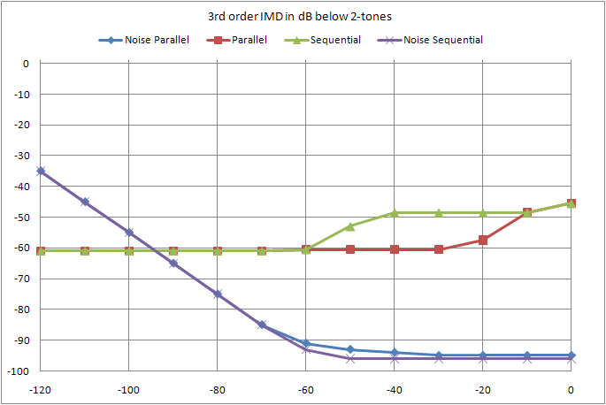
The green series "Sequential" shows the IMD3 in pure sequential mode. The purple series "Noise Sequential" shows the noise floor when measured in 10Hz RBW. In case the IMD is below the noise, the values are not measured but simply copied from the first value that was measurable above the noise. The IMD in sequential mode is excellent at -61dBc up to around -60dBm input signal. However above -60dBm, IMD quickly increases to only -49dBc at -40dBm and even -46dBc at 0dBm. A signal of -60dBm is a pretty strong signal of S9+13 but it is regrettable that the IMD increases noticeably for those stronger signals where the signal to noise ratio allows for good audio quality! AD600 is specified at -60dBc IMD for 1V output 2-tones, so it should be possible to improve on this first result.
It looks like the first AD600 amplifier in the chain is getting too much signal and produces excess IMD. This happens only at signal levels where the signal to noise ratio is already at its maximum. So a reasonable experiment is to implement Parallel Mode for the first two stages and using Sequential Mode only for the last stage. Above -60dBm the signal to noise ratio is already so good that the worsened noise figure of the first AD600 in that case is probably largely insignificant.
The blue "Noise Parallel" and red "Parallel" series show the result of paralleling the gain control for VGA1a and VGA1b. The signal to noise ratio is affected marginally but the IMD in this case is much better for > -60dBm signals. For this reason paralleling of the gain control of stage 1 and 2 is used on the Variable Gain Board. Unfortunately with signals above -20dBm the goal of -60dBc IMD or better cannot be met, but how often do we listen to -10dBm or even 0dBm in-channel signals in practice?
Signal to Noise Ratio
The noise curves in the previous graph do not directly show the signal to noise ratio as they are measured in 10Hz bandwidth. However they can be easily related to that. Just add 10⋅log(2400/10) = 23.8dB for SSB and the ultimate S/N comes out at around 95 - 24 = 71dB. The IMD together with the noise floor in 2400Hz bandwidth is shown in the following picture:
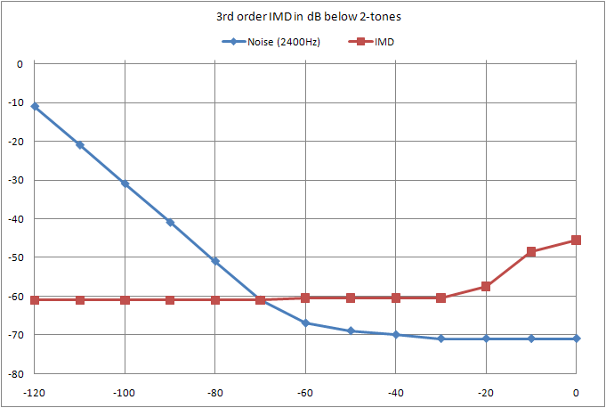
From -70dBm (S9+3dB) and upwards the IMD level is above the noise power in SSB bandwidth. Except for the strongest input signals, the AD600 IMD is not that much stronger than the noise floor. This shows that the AD600 is close to optimum with regard to IMD and S/N. The IMD introduced by AGC loop action is not shown here and is discussed separately in Closing the Loop!
Conclusion
The "good old" AD600 VGA is still the best choice given the requirements of the Variable Gain Board. Although its price tag is a disadvantage and the claimed NF by ADI is certainly not realistic, its overall performance is impressive, especially if a combination of sequential and parallel gain control is applied. The open-loop IMD3 of the signal path is below -60dBc for most of the gain control range, which matches the performance of the Selectivity Board and the goal to keep IMD below -60dBc inside the channel. One of the key features of all X-AMP VGA's is the precise linear in dB gain control, resulting in an equally linear dB/V AGC characteristic.
Please follow the links below to read more about the Variable Gain Board.
Signal Path
Control Path
Closing the Loop
Set-point Reference
Back to Variable Gain Board
Back to the TOC
|