Low Noise Amplifier
The gain block preceding the switches and quality filters on the selectivity board serves one purpose: To provide sufficient gain combined with a low enough noise figure to pin down the receivers cumulative noise figure making it independent of the insertion losses of the quality quartz filters that follow. At the input of the selectivity board, the signal is at its lowest level in the signal chain as only losses have been introduced so far. These are:
-
Antenna band-pass filter insertion loss. (1.5dB)
-
H-Mode mixer conversion loss. (5.0dB)
-
Roofing filter insertion loss. (1.0dB)
Theoretically the receivers NF could be as low as 7.5dB on most bands with this configuration, provided that no more additional loss or excess noise is introduced at this point in the signal chain. This sets the bar quite high for the low noise amplifier (LNA) on the selectivity board!
In order to obtain a cumulative NF of around 9dB for the receiver, the NF of the LNA should not exceed 1.5dB. Apart from this desired very low NF, the IMD3 performance of the LNA should be quite good also. We are protected behind the roofing filter, so "stellar" IMD performance is not needed anymore, but an OIP3 better than +30dBm, preferably better than +36dBm is needed to match the IIP3 of the quality filter that follows on the selectivity board. Let's summarize the requirements for the LNA:
-
NF < 1.5dB.
-
OIP3 > +36dBm.
-
10db < Gain < 14dB.
-
Reverse isolation > 30dB.
10dB gain is needed at least to compensate for the losses in the quality filters. Especially narrow CW filters can introduce significant loss. More than 14dB gain however is not desirable as this will limit the in-band dynamic range due to the higher than needed signal level passing the quality filters. These filters will cause the bottleneck with respect to in-channel IMD. A reasonable amount of reverse isolation is desired to shield the frontend from the effects of the steep skirts of the quality filters as much as possible.
There is no monolithic gain block available today to my knowledge that covers all requirements together at the frequency of interest: 9MHz. Some MMIC's come close, but are specified for microwave frequencies only and have a deteriorated noise figure at HF.
A relatively simple circuit with inexpensive discrete components can do it all luckily. It was Bill Carver, W7AAZ, who first experimented with paralleled J310 JFET's in source gate transformer feedback topology. He came up with the well known "Quad JFET" gain block. It has been successfully used in CDG2000 with exactly the same purpose positioned between the roofer and the quality filter. The detailed schematic of the quad JFET amplifier used here is shown below:
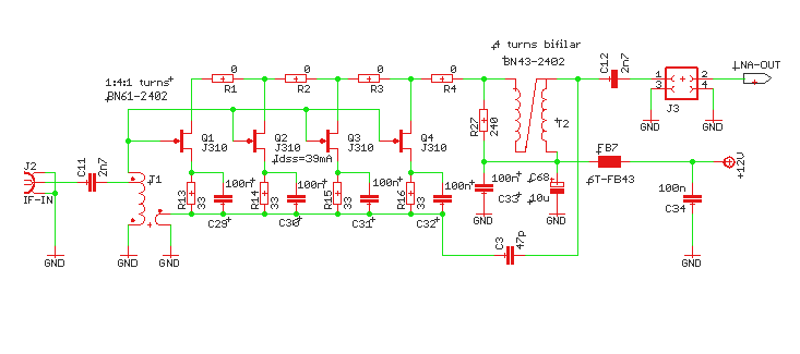
A couple of refinements have been applied to come to this version of the amplifier. One of my goals was to further miniaturize the circuit layout, without hurting its specs. Experimenting has been done with the following aspects of the amplifier to get the best out of it:
-
Source Gate Feedback Transformer.
-
Neutralization.
-
SMT J310.
-
Output Step Down Transformer.
The following paragraphs describe the tinkering with the Quad JFET amplifier in more detail.
Source Gate Feedback Transformer
The source gate feedback transformer is using the popular 1:4:1 turns ratio for this design. That is 1 turn for the source loop. 4 turns on the input to ground and 1 turn from the input to the gates. This sets the input impedance close to 50Ω given the combined transconductance of the 4 JFET's. In the original recipe the transformer is implemented with a BN61-202 ferrite balun core. The BN61-202 is relatively big (at least in the SMD world) and I liked the idea of using the much smaller BN61-2402 ferrite balun core. For best results with the bigger BN61-202 core, the single turn source winding has to be constructed as a coaxial loop through which the 5 other turns are routed. This maximizes the coupling to nearly 100%, which minimizes the losses in the feedback and that minimizes the NF of the amplifier. With the much smaller BN61-2402 core a coaxial loop, though still possible, is much harder to do and I wanted to find out if the coaxial loop could be optimized away without significant loss of performance. The idea is that if the holes in the balun are largely filled with the windings, then the coupling will be close to perfect too.
Another question mark rises around the difference in AL values between the 2 cores. The 2402 has much lower AL value than the 202 and that will affect the performance at the low frequency end of the spectrum. It has to perform well at 9MHz! So maybe BN43-2402, which has higher AL value, should be used to miniaturize the Quad JFET design.
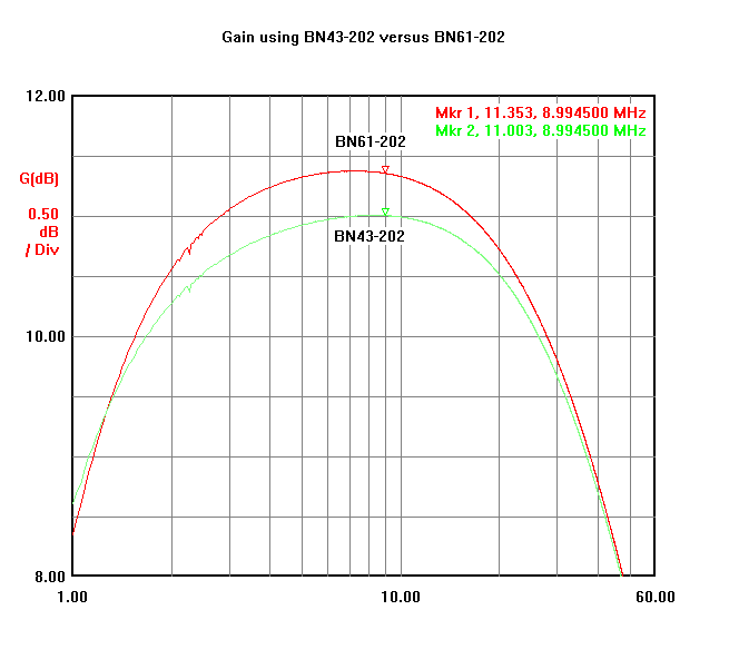
The result of experimenting with BN61-2402 and BN43-2402 cores for the feedback transformer has led to a very simple recipe for this transformer: Use relatively thick 0.7mm enameled copper wire for the single secondary loop and 0.3mm thinner enameled copper wire for the 5 primary turns. This will fill up the holes of the smaller core effectively. The core MUST be a 61 type ferrite core! Type 43 material has about 0.4dB more loss at 9MHz in this application and in the feedback transformer this will add directly to the NF of the amplifier! This confirms the use of the 61 material for this transformer in the original recipe for the amplifier by Bill Carver. Below are plotted the gain versus frequency graphs of the amplifier for both materials. The gain shown in the plot below is slightly less than shown in the other graphs on this page. The reason is that the resistor at the primary of the output transformer is 200Ω rather than 240Ω in the graph below.
In practice an increase of about 0.4dB of the NF of the amplifier could be measured in a worsened MDS by the same amount in the receiver. Unfortunately at this point in time I don't have means yet to directly and accurately measure the NF of amplifiers.
The use of the smaller BN61-2402 core with the simplified winding recipe versus the usual BN61-202 core with the coaxial loop turned out to be quite successful. The following graph plots the gain of both configurations. Also the NF in both cases is identical as no changes in the MDS of the receiver could be observed.
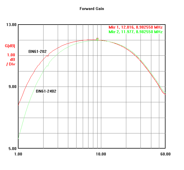
The bigger BN61-202 core gives the expected better low frequency response. The application at the IF of 9MHz however is not compromised by the BN61-2402 core. Although the difference is minimal, the bigger core is slightly worse at the high end of the spectrum which is following intuition.
The end result of this exercise is that the small BN61-2402 balun core with thick wire secondary turn and thin wire primary turns for the feedback transformer is successful at 9MHz. Therefore the BN61-2402 has been used in the feedback transformer for the remainder of this page.
Neutralization
The 47p capacitor from the output to the JFET sources neutralizes the amplifier. If the correct amount of neutralization is applied it will enhance especially the reverse isolation property of the amplifier. Reverse isolation in this application is needed to minimize the effects of the steep skirts in the crystal filter impedance connected to the output of the amplifier seen from the input of the amplifier at the frontend output. The value of 47p turns out to be the optimum value and is not very critical. A trimmer could be used to find the best value, but 47p is ok for the JFET's used. The effect of this capacitor to the reverse isolation of the amplifier is shown in the following graph:
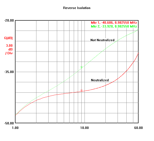
A significant improvement at the higher frequencies is seen, but also at 9MHz by about 7dB! What else is neutralization good for? The following plot shows the effect of neutralization with respect to forward gain. There is a noticeable though not stellar improvement for the high end of the spectrum:
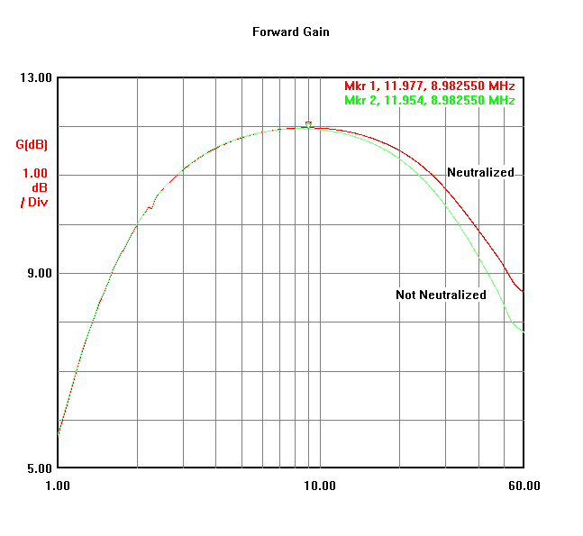
How about the input match? The following plot shows input return loss in both situations. There is a consistent 7dB improvement above 13MHz. However the optimum at 9MHz moved up to 13MHz!
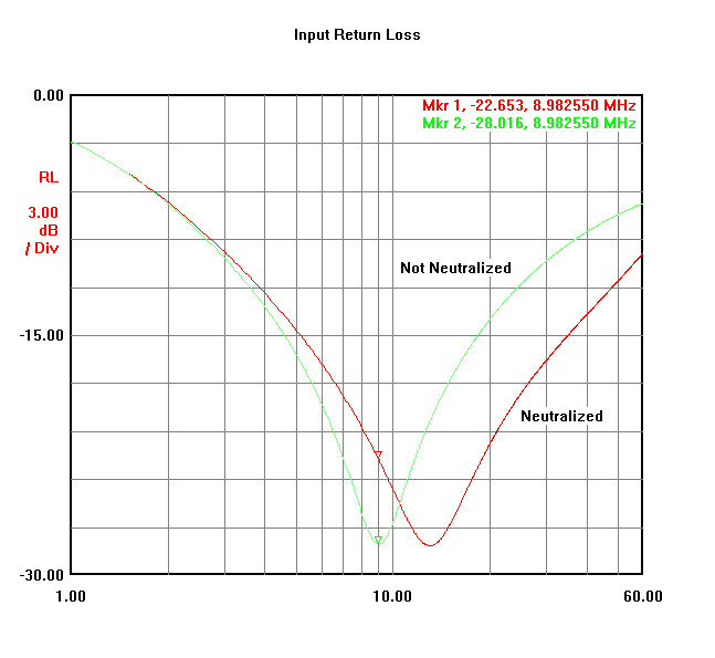
Would it be possible to get the return loss notch back right at 9MHz? It probably would be there if the input transformer where resonant at exactly 9MHz. However it is resonating at a higher frequency, so tuning it down by adding parallel capacitance is an option. The following plot shows the input impedance and its resonance at 13Mhz:
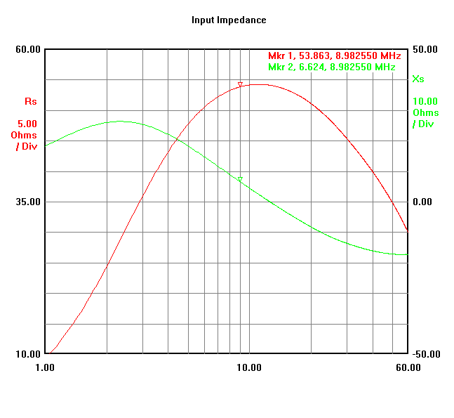
The plot shows that the input impedance is 53.8Ω in series with 6.6Ω reactance. Tuning the resonance down to 9MHz has not further been attempted as the -22dB return loss is quite sufficient already. Part of the problem is also that the resistive part is not exactly 50Ω at 9MHz in the first place. In fact this touches a more difficult issue with the Quad JFET amplifier. Its input impedance is inverse proportional with the effective transconductance of the paralleled JFET's. The transconductance increases with higher drain source current. However also temperature increases with higher current and that effectively reduces the Ids and transconductance. During initial warm-up of the JFETS after a cold start the Rin increases 5 or 6 Ω from the optimum 50Ω to over 55Ω. It requires active cooling to keep the temperature of the JFET's low enough to maintain its perfect Rin! In practice a return loss of -22dB is sufficient and no further effort is spent on the input match.
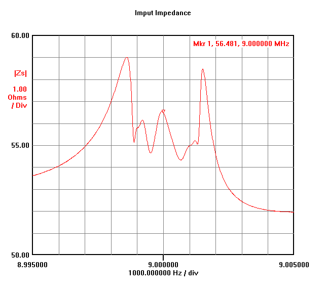
In reality the amplifier is not terminated with a perfect 50Ω resistive load. The switched-in crystal filter will provide a highly reactive load outside the pass-band especially at the skirts. The following graph shows the modulus of the input impedance seen in a 10KHz span at 9MHz when the amplifier is terminated with the #2310 2400Hz SSB filter. The effect of the skirts is still visible but reduced from kilo-ohms to just a few ohms thanks to the good reverse isolation of the amplifier. Within the pass-band the |Zs| hovers around 55.5Ω providing a VSWR of 1.15 to the output of the frontend board.
J310 JFET's
The J310 is an excellent and very affordable small signal RF device and has been around for a long time and hopefully will be for a long time from now. It is however a through-hole part in TO92 package and some day that version might be declared obsolete. Some vendors, Fairchild, OnSemi, NXP, also ship an SMD version of the old J310 and it is labeled MMBFJ310 in a SOT-23 package. To make the board layout of the Quad-JFET as small as possible the MMBFJ310 is an obvious choice to try out.
Maximum gain and 50Ω input impedance with 1:4:1 transformer all rely on a high transconductance. Also IMD is less with higher Ids. But transconductance of JFET's can vary a lot between even devices on the same strip. So I bought 50 NXP JFET's and 50 OnSemi JFET's and the approach is to select the ones with the highest and best matched transconductance. An easy way to do that is to test the Idss, which is the Ids for Vgs=0. and Vds a few volt. It turned out that the NXP JFET's where very inconsistent with Idss and the majority had quite low Idss. The OnSemi ones were much more consistent and from fifty I could easily obtain 2 matched quads with Idss=39mA. The best ones had 42-43mA but too few to form a quad. The four 33Ω resistors in the schematic set the individual Ids of the JFET's. With this value and after a warm-up time the Ids stabilize around 21.8mA per device. At 12V Vds that is 250mW to dissipate. The SOT-23 version is limited to 350mW, while the TO92 version can handle 625mW. This is a disadvantage of the SMD version. At 250mW it feels too hot to be good for the device in practice. An obvious solution is to lower the Vds, but this also lowers the IP3 of the amplifier significantly, so that is not an option. The alternative solution is to glue a piece of aluminum or copper to the 4 JFET's as a heatsink.
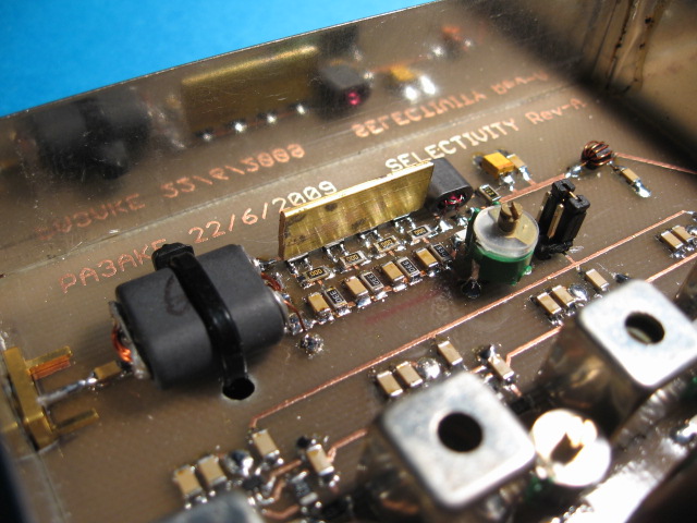
I guess this is a trick that only homebrewers can / will do! The glue is a heat conducting 2 component epoxy glue found in the better computer shops for the hardcore computer over-clocker. The metal is a piece of brass. Aluminum or copper are better, but the thermal resistance of the SOT23 case is probably the limiting factor anyway. Very little glue must be used as it is electrically conductive. This is an early version of the selectivity board with the feedback transformer still made with a bigger BN61-202 with coaxial turn and a trimmer for the neutralization. With this extra bit of cooling the JFET's are not getting too hot anymore and the Zin drops to about 53Ω.
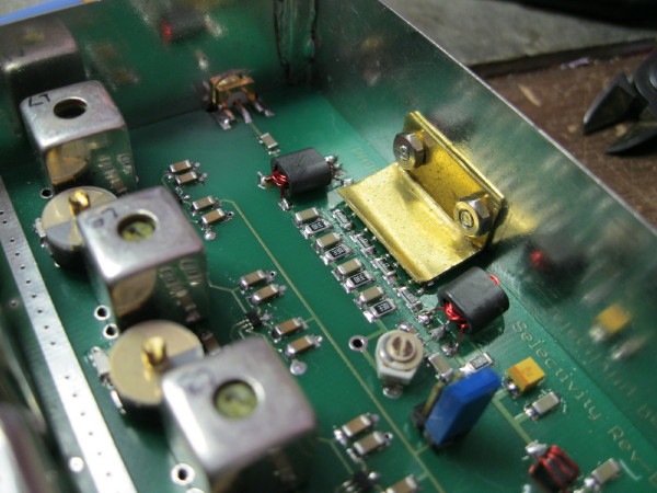
An alternative cooling approach is provided to me by Dan Ray, AC6AO, which avoids the glueing all together, and which will provide even better cooling if the heatsink is pressed firmly on all the 4 JFET's. See the picture below:
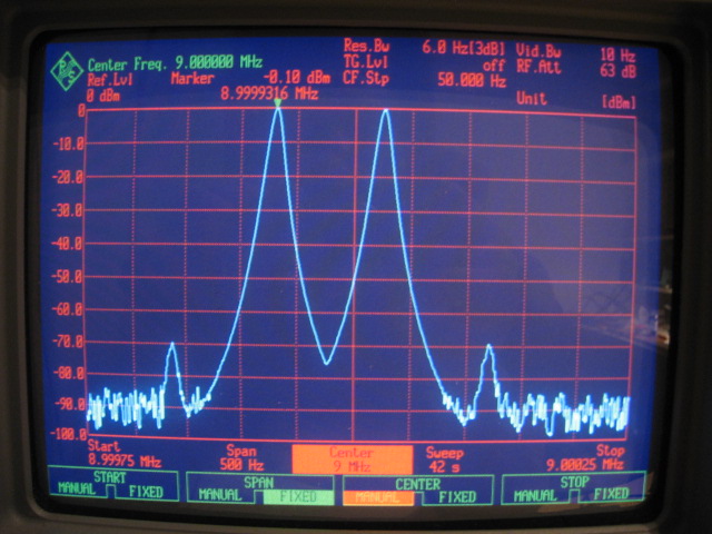
The OIP3 measured with the Quad JFET amplifier using the OnSemi devices running about 22mA each at 12V is +35dBm. This value is sufficient at this position in the signal chain to ensure that the quality filters on the selectivity board will cause the in-band IMD bottleneck of the board. The following picture shows the IMD contributed by the amplifier at 0dBm output level. There is no difference between using a BN61-202 or the smaller BN61-2402 ferrite core in the input feedback transformer. Apparently the non-linearity is caused by the JFET's alone and not the ferrite.
Output step down transformer
The final tuning of the original design has to do with the output transformer. The CDG2000 recipe for this transformer prescribes 5 bifilar turns on a BN61-202 balun core. With the result obtained with the feedback transformer the obvious idea is to also use BN61-2402 at this position simply to reduce space. But why not use BN43-2402? The 61-ferrite is not a must for the output transformer. A little bit extra loss when using 43-material is not a problem here as it will not add directly to the NF of the amplifier. The good reason to use 43-ferrite in the output transformer is that it effectively suppresses parasitic oscillations in the VHF region, which otherwise the Quad-JFET is prone to. The 43-material becomes much more resistive at VHF than 61-material. In the original Quad J310 design the parasitic oscillations are suppressed with a small 43-material bead around each drain leg of the J310. It turns out that the circuit is also completely stable with the BN43-2402 output transformer without the ferrite beads. Also the elimination of the ferrite beads slightly increases the gain and that compensates for minimal extra loss in the output transformer.
The output transformer is a critical component in the Quad-JFET circuit. The reason why the gain drops off considerably above 50MHz is due to the capacitive loading of the JFET's drains with the transformer. The gain bandwidth can be extended considerably with a different output circuit. An NPN transistor in cascode with the JFET's does significantly extend the bandwidth at the high side at the expense of a higher supply voltage and dissipation. This technique does not help to improve the input match over a wider frequency range though. I have only simulated the cascode variation. No prototypes have been build. For the 9MHz narrow band IF application it is not really needed.
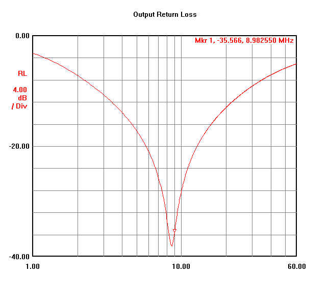
The return loss plot of the output is shown in the following picture. It shows a near perfect -35dB at 9MHz. This is not completely by accident. The output transformer allows some freedom to play with the number of bifilar turns. With the BN43-2402 binocular core, 4 turns of bonded wire produce output resonance very close to 9MHz. With a 240Ω loading resistor at the primary side the output resistance is also set very close to 50Ω as the return loss picture shows. Unlike parameters such as forward gain, reverse isolation and input impedance the output impedance is not affected at all by neutralizing the amplifier.
Conclusion
The Quad JFET gain block with its very low NF of around 1.3dB and good OIP3 of +35dB is a perfect choice to provide the first amount of fixed gain in the signal path between the roofing filters and the quality filters. Its good reverse isolation of -40dB when neutralized at 9MHz helps to shield the crystal filter reflection outside the pass-band. With the 1:4:1 feedback transformer ratio and 22mA per JFET the input impedance is close to 50Ω and the gain is 12dB, which is just about right in this position. At the output the amplifier is closely matched to 50Ω. The amplifier can be made with a rather small layout with the help of SMT parts and the much smaller BNxx-2402 balun cores. BN61-2402 should be used at the input. BN43-2402 should be used at the output. The weakest point of the amplifier is the dependency of the Zin and forward gain to the temperature of the JFET's. With the SMD version a small heatsink is recommended to keep the temperature of the 4 devices at an acceptable level, without decreasing Vds and sacrificing the IP3.
There is a detailed theoretical discussion of the source gate transformer feedback JFET amplifier in Wes Hayward's excellent book "Introduction to RF design". The obtainable NF of the amplifier can be modeled with the following formula: F=1+Rt/Rs. Rt represents the internal noise source caused by the 1/gm source impedance of the JFET and Rs is the external source resistor. Rt is about 18Ω with the 4 J310's in parallel at 22mA each. Rs is 50Ω. So the theoretical approximation of the best obtainable NF = 10*log(1+18/50) = 1.34dB. This seems to be possible in practice! For those interested in the math behind the Quad JFET amplifier, Wes Hayward's theoretical analysis of the amplifier is well worth reading.
Filters
Switches
Pre-Amplifier
Back to Selectivity Board
Back to the TOC
|