Introduction
The AGC system described here provides both a traditional Attack/Decay AGC strategy as well as a Hang AGC strategy. Depending on how it is set up by the operator the system will be in Attack/Decay-Mode or in Hang-Mode or in a combination of both! Because Attack/Decay-Mode is preferable for weak (CW) signals and Hang-Mode is preferable for strong (SSB) signals the system can be configured to automatically provide Attack/Decay-Mode for signals below a certain average signal level and Hang-Mode for signals above that threshold.
There is sufficient board space on the euro-card sized board to implement the extra functionality of the dual behavior AGC. This is possible thanks to the simplification of widening the noise bandwidth of the signal path from 2.7KHz to 212KHz resulting in the elimination of the crystal noise filter and one of the two detectors in the original design. This simplification also results in much increased loop stability!
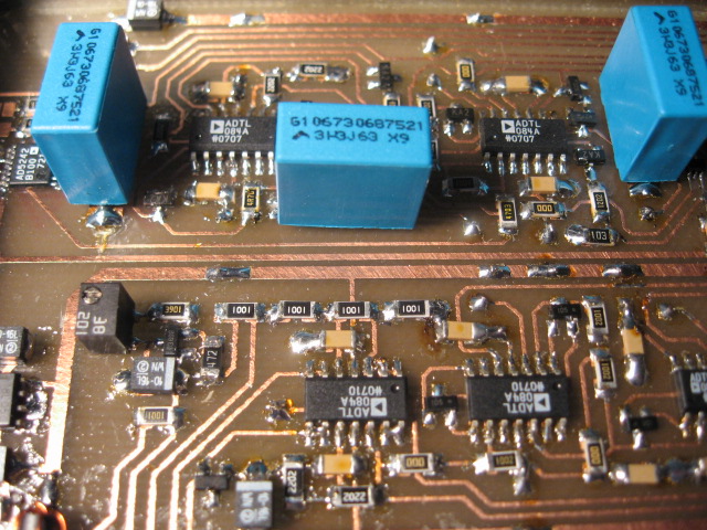
There is however still a FAST path and a SLOW path, but only using one detector! Below is a close-up picture of the AGC timing part of the Variable Gain board. The three big blue foil capacitors provide the time constants of the Attack, Hang, and Decay phases. The bottom half of the picture shows the main reference voltage and its various derivations.
Control Path Block Diagram
The following picture shows the block diagram of the AGC control path of the Variable Gain Board. The 9MHz signal path has been left out in order to focus on the details of the control path.
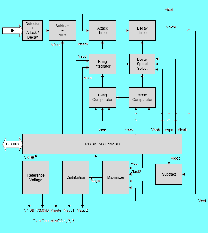
The next sections will describe the individual blocks and how they cooperate in more detail. Frequently there will be references to parts on the schematic, so it is a good idea to have a printout of Sheet 3 and Sheet 4 of the schematics available.
I2C Control
The board is fully controlled by means of I2C logic. This functional block is depicted as the central "I2C 8xDAC + 1xADC" block in the diagram and consists of IC16, IC17, IC18 and IC19. The following voltages are set with IC18 and IC19 (AD5306 4-channel 8-bit DAC):
-
Vfloor, Vhth, Vath, Vsph, Vspa, Vleak, Vloop, Vgain
A dual 8-bit digital pot-meter AD5242 IC16 is used to control the following parameters:
The AD5242 also features two general purpose output bits, which are used to set the following control signals:
The above twelve I2C controlled set-points completely parameterize the behavior of the AGC control path. The exact purpose of each set-point will be explained in more detail later on this page. Also a set-point reference manual is given in Set-point Reference.
Apart from the reference voltage, the I2C block has only one analog input signal called Vagc. This is the AGC's output control voltage that ultimately sets the gain of the signal path. Vagc is digitized with IC17, AD7999, an 8-bit ADC, to be used for an S-meter implemented in software.
The 9MHz signal path output labeled VDET-IN on the schematic enters the Detector block at the top left of the diagram. The Detector consists of a diode voltage doubler rectifier with a pair of Schottky diodes D16. The circuit features a fairly fast and fixed attack and decay time constant. These 2 time constants set the dynamics of the FAST path and should be fast enough to follow the envelope of any practically possible input signal fed into the Variable Gain Board. In practice the maximum input signal envelope rise time is set by the group-delay of the crystal filter selected on the Selectivity Board.
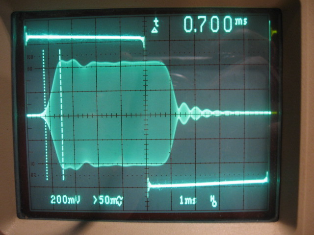
The following picture shows the step response of the INRAD 2.4 KHz 8-pole SSB filter on the Selectivity Board. A 9MHz carrier is switched on and off using a pair of FSA3157 SPDT switches with a 1 KHz square wave and fed through the filter to obtain this picture. The group-delay at the center of the SSB filter is measured at 700μs, see Selectivity Board Filters for details.
The picture shows that the envelope of the output signal takes 1.5ms to arrive at its maximum. This is about twice the measured group-delay. The attack time of the FAST path has to be set such that Vfast is just able to keep up with the ramp-up during the 1.5ms delay of the SSB filter. This guarantees a linear mode of operation of the signal path if no wider (faster!) than 2.4KHz crystal filters are used on the Selectivity Board.
Also note the visible ringing at 2.4KHz especially in the OFF situation! The picture suggests that the signal is completely off during the first 700μs. This is certainly not the case. Don't forget that the oscilloscope has a linear Y-scale. A logarithmic scale would be much more useful in this case!
The next picture shows the step response of the INRAD 500Hz 8-pole CW filter. The delay is almost 7ms before ramp-up of the envelope is finished. This corresponds well with twice the 3.4ms group-delay measured at the center of this filter. The ringing in the OFF situation seems to be less severe than with the SSB filter, although the 1KHz switching is a bit too fast for a good observation.

The diode detector output voltage is buffered with IC10C. Next in the control path is IC5B which subtracts Vfloor from the detector output signal. A gain of 10 is also applied to bring the AGC control voltage within the range needed by the AD600's in the signal path. Vfloor is set through I2C in software. It resembles the average output voltage of the detector with no input signal at maximum gain, caused by wide-band noise in the signal path. The subtraction of Vfloor from the detector output results in an AGC control range starting from near 0V, usually at about 300mV. Vfloor is used in the important adjustment that precisely sets the end of the control range at the largest input signal that can be swallowed by the signal path: +3dBm.
The diode detector output voltage is called Vfast and it is the FAST path AGC voltage also used to derive the SLOW path Vslow from. The direct purpose of Vfast is to quickly respond to any signal level change, keeping the signal path in a linear mode of operation all the time, preventing transient distortion.
Attack and Decay
The Attack and Decay blocks are used to condition the Vfast control signal into the Vslow control signal. In most analog AGC systems, attack and decay time constants are derived from a single passive network consisting of multiple R's and C's. In this design the attack and decay time constants of the SLOW path have been completely isolated from each other into two separate blocks. Each block is using its own storage capacitor and the means to charge and discharge it. This makes independent control of each time constant over a wide range much more accurate and simple.
The Attack block has an I2C configurable RC time constant made up with the digital pot-meter IC16 + R61 and C64. The output clamp providing the isolation from the Decay block consists of IC6A and D2. The RC product is ranging from 70ms to 400ms. This fairly slow attack time of the SLOW path has two purposes.
-
It allows for good short signal spike handling. Short spikes can ramp up Vfast quickly as the attack time of the FAST path is only about 1ms. This keeps the signal path in its linear region, preventing short lasting though serious transient distortion. However the maximum decay time of Vfast is only 70ms, which is less or equal to the minimum attack time of Vslow, and hence Vslow will not pick up the Vfast pulse if its duration is short enough! This prevents a long loss of sensitivity by not unnecessarily triggering Vslow. This behavior helps to deal with certain types of QRN.
-
Maybe the more important purpose is to minimize gain modulation IMD. Gain modulation IMD and how it is dealt with is a separate subject discussed in more detail in Closing the Loop.
The 22KΩ resistor R61 is there to guarantee that the attack time of the SLOW path will never be less than the decay time of the FAST path. This is an important detail because this prevents instability of the FAST path that otherwise can occur by interaction of the timing of the FAST path and the SLOW path.
The Decay block is slightly more complex than the Attack block. Instead of using a Voltage-RC based time constant, this circuit uses a voltage controlled current sink to discharge decay capacitor C65. The advantage of this approach is that the increase in signal path gain during the decay phase can be expressed in a constant dB/s over its entire control range and is linear over the entire control range. It is therefore more convenient to talk about Decay-speed rather than Decay-time.
The complete Decay block consists of IC6B, IC6C and IC6D and surrounding components. IC6D is used to subtract the output voltage from the "Decay Speed Select" block, pin 4 of IC14, from the voltage over the decay capacitor. Therefore the voltage over R77 is always equal to the speed select voltage, turning it in a voltage controlled current sink that discharges the decay capacitor with a current independent of the voltage over the capacitor.
Given the 3.3uF, the 33KΩ and 5V maximum voltage, the Decay block is capable of a maximum decay speed of 45.91V/s. With the 33.67dB/V of the signal path this gives 1546dB/s. This translates into 84.8ms for a decay from minimum gain to maximum gain at its fastest setting. The DAC used for the speed select voltages has 8-bit precision, so the decay speed can be controlled with a step size of 6.06dB/s from 0dB/s to 1546dB/s.
The decay circuit uses 0.1% precision resistors to make sure that C65 will never charge up through R77. To be absolutely sure also with some unlucky OPAMP offset voltage, IC6C has been added to provide a clamping action such that this cannot happen ever. The clamping function should be redundant, but see it as insurance. With a 6.06dB/s step size, the first position after the not so useful "infinite" decay time is 21.6s total decay time from minimum gain back to maximum gain.
Maximizer
Before diving into more detail on how the Attack/Decay versus Hang AGC strategy is applied, let's have a look at how the FAST path and the SLOW path are combined to produce the Vagc control signal. This is the function of the "Maximizer" block. It is implemented with IC8A, IC8B, IC8C, IC8D, IC11A and IC11B. It has 4 inputs: Vfast, Vslow, Vgain and Vext. The output, Vagc, is always the largest value of the 4 inputs. So the strongest control signal controls the gain of the signal path. Vgain is an I2C DAC supplied voltage that is used to set the maximum gain manually with software, usually called the IF-gain or RF-gain control. Vext is an optional external analog input that can be used for instance to configure two receivers in diversity reception. Vfast and Vslow represent the FAST and the SLOW AGC path.
The block diagram shows that actually not Vfast but Vfast2 enters the maximizer. Vfast2 is Vfast but with Vloop subtracted. Vloop is a small voltage supplied by the I2C block. The result of this detail consisting of only IC5C and four precision resistors is significant. It helps greatly in reducing IMD produced by gain modulation, which is described in more detail in Closing the Loop. In short, the Vfast control voltage only defines the gain for a short time as it will be pushed away by the slightly larger Vslow when Vslow reaches the end of its attack time. Vslow has a much larger attack and decay time, and hence the loop bandwidth is much narrower. When Vslow takes over gain control, the IMD produced by AGC gain modulation will be considerably less as it falls outside the loop bandwidth!
Distribution
The Distribution block uses Vagc to pass the gain control voltage to the four AD600 VGA amplifiers. IC9C and precision resistors R75 and R76 are used to divide Vagc by two in order to drive the gain control of IC1 and IC2 in parallel but each with the half the dB/V. This minimizes IMD at the very strong signal end of the control range. AD600 is expensive and does not survive plus or minus 12V on its control pins, so clamping diodes D12, D13, D14 and D15 are used to ensure that an error in the AGC control voltage will not become catastrophic for the AD600's.
IC9D on the schematic provides a buffered VAGCOUT voltage which can be used to drive a conventional electro-mechanical S-meter. Another application is to use it as Vext for a second IF strip in diversity reception. There is a disadvantage however in using VAGCOUT directly without further processing for an analog S-meter. Below the AGC threshold, the scale will not follow the perfectly linear 32dB/V of the AD600. The 8-bit I2C ADC IC17 provides a more versatile way for accurate S-metering. First of all the non-linearity of the scale below the threshold can be compensated for in software. Second, in software it will be quite easy to compensate also for changes in frontend gain that come with different frontend configurations. One can think of the differences in insertion loss between CW and SSB quartz filters, antenna BPF filters and optionally switched in pre-amplifiers or attenuators. Using the digitized Vagc will allow for precise calibration of the S-meter independent of the frontend configuration. This turns the receiver into a selective level meter, accurate to 1dBm over an impressive 120dB signal level range!
The Reference block provides precise reference voltages needed by the other blocks. The various voltages are all related to the AD600 gain control requirements. We need the following precise voltages:
-
0.649V
This voltage is labeled V0.65B in the schematic. It is needed to configure the gain control interface of IC3 in sequential mode such that gain reduction begins at 0V AGC voltage. So the AD600 pair at the end of the chain is the first to reduce its gain.
-
1.298V
This voltage is labeled V1.3B in the schematic. It is needed to configure the gain control interface of IC1 and IC2 in parallel mode such that gain reduction of IC1 and IC2 begins when IC3 has reached the end of its control range.
-
3.894V
This voltage is labeled V3.9B in the schematic. It is needed as the reference voltage for the I2C DAC IC18 and I2C ADC IC17. The 3.894V exactly specifies the end of the AGC control range, which allows the DAC's to provide voltages up to that value. The same applies for the ADC. It can digitize the full AGC control range using all 8 bits
These three reference voltages are all derived from a precise programmable shunt reference IC15. This is done with precision resistors and the OPAMP's IC9A, IC9B and IC10D. The reference is adjusted to exactly 2.596V with a 10 turn trim-pot R88. This trace is labeled V2.6U in the schematic. Apart from the inductor of the noise filter in the signal path, this is the only analog alignment needed to setup the Variable Gain Board. All other alignments have either been eliminated through robust circuits that don't need alignment or are dealt with by the I2C DAC's controlled through software.
Decay Speed Select
The blocks Mode Comparator, Hang Comparator, Hang Integrator and Decay Speed Select together define the AGC strategy and have close interaction with each other.
The Decay Speed Select block is used to select the appropriate decay speed of the Decay block depending on the current AGC strategy. It selects one out of three preset speeds which are provided with the I2C block DAC's. These presets are:
-
Vspa
Vspa is selected in Attack/Decay-Mode. Vspa defines the decay speed during the decay phase of Attack/Decay-Mode.
-
Vleak
Vleak is selected in Hang-Mode when the AGC is in its HANG state. It is called Vleak as it defines a very slow decay speed allowing the AGC to follow slow QSB.
-
Vsph
Vsph is selected in Hang-Mode when the AGC is in its DECAY state. Usually the decay speed in Hang-Mode is quite fast to quickly regain sensitivity when the HANG state has expired.
The Decay Speed Select block consists of IC13 and IC14, a pair of FSA3157 SPDT switches in the schematic.
Mode Comparator
The Mode Comparator block in the block diagram is the block that selects the current AGC strategy. The current AGC strategy can either be Attack/Decay-Mode or Hang-Mode. The AGC level represented by Vslow is used to decide which mode is used. When Vslow is below the threshold defined by Vath the AGC will operate in Attack/Decay-Mode. When Vslow is above Vath the AGC will operate in Hang-Mode.
Vath is defined through software with a DAC from the I2C block. With this mechanism the AGC can be configured to always use Attack/Decay-Mode if Vath ≥ 3.894V. If Vath ≤ 0V the AGC will always use Hang-Mode. For any other value of Vath in between these two extremes, the actual AGC level and Vath will set the current AGC mode. The Mode Comparator block consists of IC5D and D1 in the schematic.
Hang Integrator
The Hang Integrator block defines if the Hang AGC is in its HANG state or in its DECAY state and it provides the integration time constant that sets the maximum hang time. The circuit consists of IC7A, IC7B and IC7C in the schematic. The integrator itself is made with IC7C.
When the output of the integrator is below 0V, the AGC is in its HANG state and Vleak is selected with the Decay Speed Select block. If the output of the integrator rises above 0V, the AGC changes state to the DECAY state and Vsph is selected with the Decay Speed Select block to set the speed of the decay. The direction and speed of the integration is defined by the following forces:
-
Vhot
Vhot is the strongest of the 3 integration inputs. Vhot stands for "hang-on-transmit". When Vhot is high, the integrator is quickly discharged into HANG state regardless of the current AGC strategy. So Vhot is active in both Attack/Decay-Mode and Hang-Mode. This feature is useful to maintain the AGC level constant over short transmissions keeping the receiver's sensitivity temporarily unchanged.
-
Vspd
If the outcome of the Hang Comparator is low, meaning "Please Don't Hang!", the integrator is charged up towards the DECAY state. The speed at which this takes place is set by Vspd. Vspd is software controlled with a digital pot-meter in IC16 and defines the hang time of the Hang AGC.
-
Hang Comparator
If the outcome of the Hang Comparator is high, meaning "Please Hang!", the integrator is discharged towards the HANG state. With a long hang time, small Vspd value, the integration towards HANG state is fast. With short hang time, high Vspd value, the integration towards HANG state is slow. The result of this is that the HANG state is promoted by the Hang Integrator block if a longer hang time is selected.
Hang Comparator
When Vhot is low, the direction of integration of the Hang Integrator is defined by the outcome of the Hang Comparator block. This is the normal situation when not transmitting. The Hang Comparator consists of IC12, IC5A and IC7D in the schematic. When the outcome of the Mode Comparator block is high, the Hang Comparator block is simply disabled. This is the situation when the AGC is in Attack/Decay-Mode and Vspa will be selected by the Decay Speed Select block.
However when Hang-Mode is selected rather than Attack/Decay-Mode, then the outcome of the Hang Comparator depends on its 3 inputs: Vslow, Vfast and Vhth. If the sum of Vfast and Vhth is less than Vslow, then the outcome is low and the integrator will move towards the DECAY state, otherwise the outcome is high and the integrator will move towards the HANG state. Vslow represents the AGC level. Vfast represents the actual signal level. If the actual signal level is more than the Vhth threshold below the AGC level, then the integrator will time out towards the DECAY state.
Vhth is set through software with a DAC from the I2C block. Because the AGC is linear in dB, thanks to AD600's 32dB/V, Vhth defines the number of dB's the signal level is allowed to fall without beginning to change the Hang Integrator state. So Vhth is a constant "hang-window" expressed in dB's independent of the actual AGC level. This detail is different from the original design by W7AAZ, where the "hang window" is defined by a fall of the signal level to 90% of the AGC level in dB. So the lower the AGC level, the smaller the window becomes where it maintains its HANG mode. This 90% rule results in more nervous hang AGC behavior in the case of signals close to the noise floor, where the "hang-window" approaches in theory 0dB!
One more circuit detail needs clarification. When the Hang AGC is in DECAY state, IC12 is used to select 0V rather than Vhth in the Hang Comparator. This allows Vslow, the AGC level to drop almost all the way to Vfast, the actual signal level instead of the sum of Vfast and Vhth, during the DECAY state. The choice of precision resistors around IC5A is such that the gain of the summing amplifier IC5A is guaranteed to be slightly more than unity providing a small amount of hysteresis, which is necessary to re-enter the HANG state when Vslow approaches Vfast again.
Simulated AGC Behavior
A couple of SPICE circuit simulations are used to graphically demonstrate the functioning of the AGC system in pure Attack/Decay-Mode, pure Hang-Mode and a combination of the two.
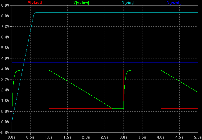
Attack/Decay-Mode
The following picture shows the behavior of the AGC in Attack/Decay-Mode. In this case Vath = 4V, so the AGC is forced into Attack/Decay-Mode regardless of the Vslow level. Vint represents the voltage at pin 8 of IC7C, the hang integrator, and Vswh represents pin 7 of IC7B, the Hang Integrator block output voltage. Note the exponential attack of Vslow and the linear decay of Vslow. Vint quickly ramps up into DECAY state and stays there indefinitely. Also Vswh is always high, which represents DECAY state. However, as soon as Vfast becomes less than Vslow decay kicks in immediately. The decay speed is set by Vspa which is 0.1V in this simulation. Note that the resulting Vagc is the maximum of Vfast and Vslow, the red and the green curve.
Hang-Mode
The next picture shows a simulation where the AGC is forced into Hang-Mode independent of Vslow by setting Vath = 0V. The same Vfast is applied and initially Vint ramps down deep into HANG state. At 1s into the simulation Vfast falls down to 1V, which is way outside the hang-window set by Vhth and now Vint begins to ramp-up towards DECAY state. When Vint exceeds 0V at 1.6s, Vswh goes high and the DECAY state is entered. Vslow now quickly decays with the speed set by Vsph until Vslow equals Vfast again at 1.8s at which point the integration is reversed. Not much later the AGC is in HANG state again and the whole cycle repeats itself from 3s and onwards.
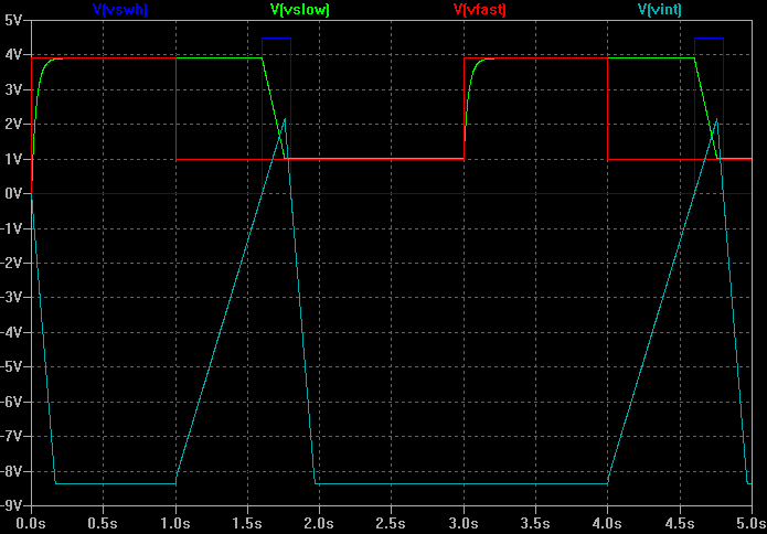
Combined Attack/Decay and Hang-Mode
The next picture shows a combined Attack/Decay-Mode and Hang-Mode behavior. A more complex Vfast is used in this example. Vfast slowly decreases but Vslow remains hung at 3.9V initially. At 1.9s in the simulation Vfast + Vhth is finally low enough to become less than Vslow. Vhth = 0.6V in this example. At that point Vint ramps up until the DECAY state is entered signaled by a Vswh going high at 2.5s. Now Vslow decays with Vsph decay speed to equal Vfast again. Again a HANG state is entered until at 3.7s another DECAY state is reached. This next DECAY state is again using Vsph decay speed until Vslow equals Vath. As soon as Vslow is less than Vath, which is 1.5V, the AGC transitions from Hang-Mode into Attack/Decay-Mode. At that point the much slower decay speed set by Vspa is used for Attack/Decay-Mode and it remains in this mode until Vslow is again greater than Vath.

Conclusion
The complete Control Path presented here is implemented from scratch with mostly general purpose components such as OPAMP's, diodes, resistors and capacitors. It is surprising (or maybe not) that today as far as I know there is no solution available in a single dedicated linear AGC-processor IC. That could have simplified things considerable! However thanks to SMD components and many hours of manual PCB routing, the entire Control Path uses only approximately 50% of the euro-card sized board, while being capable of two common AGC strategies.
Implementing the Control Path fully digital with ADC-FPGA-DAC could be a nice project and entirely possible with Verilog FPGA programming, although not much improvement on cost or board size is expected, but certainly much more flexibility!
This concludes the detailed description of the AGC Control Path. Please follow the links below to read more about the other aspects of the Variable Gain Board.
Signal Path
Control Path
Closing the Loop
Set-point Reference
Back to Variable Gain Board
Back to the TOC
|