Introduction
The Variable Gain Board can be operated in open-loop mode using manual gain control with the Vgain control voltage. Open-loop mode can be useful sometimes and especially with certain receiver measurements. However in order to save your ears, normally the board will be used in closed-loop or AGC-mode where the AGC action attempts to keep the output signal at a constant level given that the input signal is above the AGC threshold. On this page an evaluation is presented of the Variable Gain Board in the closed-loop configuration.
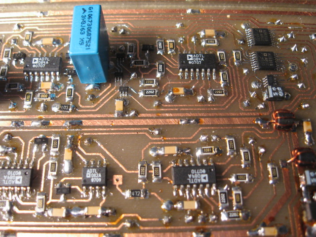
Much of the closed and open-loop behavior is controlled by means of I2C DAC's. The picture below shows a close-up of some AGC circuits. In the top right corner the two 4-channel I2C DAC IC's are visible and below that the I2C ADC IC that samples the Vagc control voltage. In the center in the shade of the bulky foil capacitor the FSA3157 switches can be seen that implement the Decay Speed Select block.
AGC Function
The following graph shows the value of the Vagc control voltage in mV versus the 9MHz input signal level in dBm in closed-loop configuration. Above the approximately -115dBm AGC threshold level, the transfer curve is almost perfectly linear with a slope of 33.67dB/V or 30mV/dB due to the near ideal 32dB/V control characteristic of the AD600. There is however a slight deviation visible from the ideal 30mV/db around -70dBm. This is the area where the transition is made from the sequentially controlled IC3 to the parallel controlled IC1 and IC2. A disadvantage of parallel control is that the linearity errors in dB/V add up. This is exactly what happens here, but not to a serious extent.
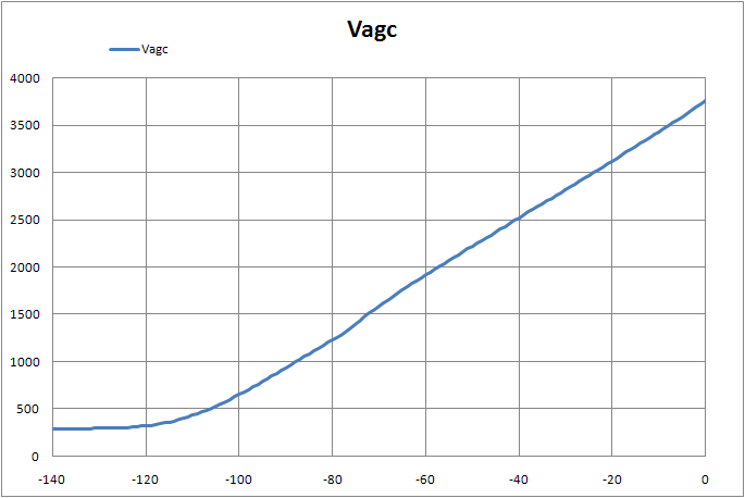
Vagc is plus minus 300mV when the input is terminated in 50Ω and no signal is applied. This represents the first 10dB of the 131dB control range so in practice 121dB gain control is available in closed-loop. Above the AGC threshold, the output voltage in 50Ω is kept close to 86mVtt thanks to the feed forward flattening function of the final AD602 VGA section in IC4. The 86mVtt output signal represents a power of approximately -17dBm. This output level is a bit too strong for a 7-level ring mixer product detector (SBL-1 and alike), but with the linear QSD detector used further down the signal path it does not need any further attenuation. The next graph shows the output level versus the input level:
The diode detector produces approximately 500mV with no input signal applied. This represents the noise floor of the AGC set by the bandwidth of the noise filter and the total closed-loop gain seen before the diode detector. At the end of the AGC range at 0dBm input signal, the diode detector produces about 865mV in closed-loop. This is an increase of 4.7dB. The gain flattening function with IC4 compensates for the 4.7dB increase of output signal at the end of the control range. From the picture we can see that it actually slightly over compensates by about 0.1db per 10dB, but that will be hard to detect by ear!
The control range inside the feedback loop is 126.4dB, so the feedback loop gain is G = 126.4 / ( 4.7 - 1 ) = 34.2 times. This effective feedback loop gain of 34.2 is provided by IC4, the diode detector, IC5B and the 32dB/V of the AD600. Given its fixed 0.1875V control voltage, the AD602 amplifier IC4 adds 16dB gain to the loop, which is 6.3 times. IC5C gives 10. This means that the diode detector has a scale factor of 34.2 / (6.3⋅10⋅32) = 17mV/dB.
The diode detector does not have a true logarithmic transfer function like the detectors used by W7AAZ in the original design. However due to the rather high loop gain of 34.2, the detector is only operating over a small part of its range in closed-loop and therefore its non-logarithmic behavior is not causing large changes in loop control dynamics over the AGC's entire 131dB control range. This aspect is not critical anyway, because of the absence of a noise filter with considerable group-delay in the feedback loop.
Although the AGC threshold at approximately -115dBm does not help with accurate S-meter readings below S2, the Vagc can still be used to provide readings below S2 in the bend of the curve. IC17, 8-bit ADC AD7999 digitizes Vagc and with software this can now be further linearized for use in a software S-meter using a lookup table that map the 256 possible ADC outcomes to the corresponding dBm values. If a calibrated signal generator is available, the software S-meter can be calibrated from -125dBm to 0dBm and from -115dBm the reading can be accurate within 1dBm! If a pin compatible 10 or 12 bit ADC is used (AD7995, AD7991) the accuracy up to 10dB below the threshold can be further improved at the cost of a larger lookup table and a bit more software complexity, but this is probably not necessary for most of us.
Loop Dynamics
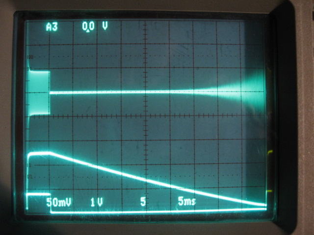
Because of the relatively wide noise filter in the signal path, the closed-loop behavior can be configured for pretty fast attack times without any signs of instability. SPICE simulation of the closed-loop shows that an attack time of 5μs is possible. To show that this is possible in practice as well, the SLOW path is disabled and the FAST path is configured with the R and C values from the simulation. The AGC response to a 100dB signal jump up and down is shown in the following picture:
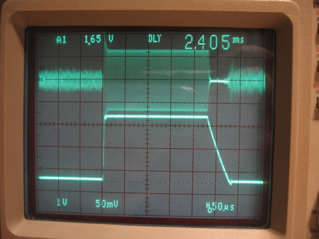
The picture shows a very stable AGC response that exactly mimics the SPICE simulation: 5μs attack and 50ms decay. However such very fast attack and decay times of the FAST path are not needed or even desired in the receiver as the group-delay of the SSB crystal filter slows the signal rise time down to about 1.5ms at minimum. See Control Path for the pictures!
An attack time of around 1.5ms is fast enough to follow the fastest input signal jump. The following picture shows the response of the slowed down FAST path to a 5ms pulse of -40dBm input signal. This is again with the SLOW path disabled. The output signal together with the Vfast response and the pulse that switches the input signal on and off are shown below:
As expected the result is a stable and far slower AGC response. The decay phase now lasts about 45ms. Its exact speed depends on C36 (220n), R86 (560K) and last but not least the 500mV noise floor of the detector. The decay operates over the relatively linear first part of its exponential RC decay curve, because of the always present 500mV closed-loop detector floor. The decay speed is fairly constant at approximately 50V/s which translates to 1600dB/s. With this speed the maximum decay time over the entire 131dB control range is 80ms.
The following picture zooms further in to show the attack phase in more detail:
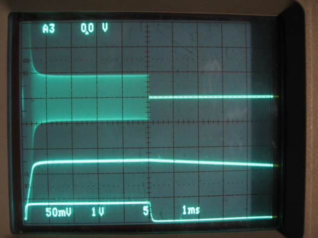
The attack phase only lasts 500μs, which is a lot faster than expected from R47 (10K), C36 (220n) and the 500mV detector floor. The reason for this is the temporary overload of the signal path, which gives a lot more voltage from the diode rectifier. In reality this will be much different with the crystal filter in front slowing the ramp-up of the input signal down to at least 1.5ms.
The next picture shows the response to the same -40dBm signal pulse but now with the Selectivity Board in front with the SSB filter selected:
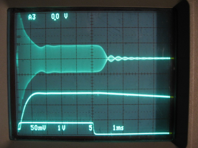
Now the attack phase lasts 1.2ms. The output signal still makes a considerable 10dB jump, but much less than without the crystal filter. The jump is short lasting and remains within range for the AD600's. There is no clipping.
The next picture shows the AGC response when the 500Hz CW filter is selected:
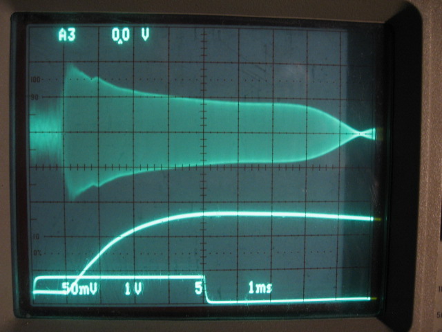
The attack phase with the CW filter lasts 5ms. This is actually the time to be expected given the component values and the noise floor. There still is a temporary 5dB overshoot in the output signal, but as was the case with the SSB filter, the AD600's always remain linear and never clip.
The FAST path allows the AGC to respond quickly to a signal jump. It responds just fast enough to prevent clipping and the associated transient distortion. The SLOW path is derived from the FAST path and is really much slower to provide the desired hang time and / or decay speed. The attack time is operator adjustable between 80ms and 400ms. The decay time is also operator adjustable between 85ms and 21.6s for the complete 131dB control range.
Unfortunately at this time I have no digital storage oscilloscope at my disposal that enables me to show a few good real-time examples of the combined behavior of the FAST and the SLOW path. Hopefully I will be able to add some pictures somewhere in the future!
AGC induced Intermodulation
AGC systems do produce IMD by design. The mechanism that introduces the intermodulation is gain modulation. If the control loop bandwidth is wide enough to pass the difference in frequency between two carriers inside the channel, then these carriers will cross modulate each other's amplitude. This produces pure odd order intermodulation! A demonstration of the principle is given with the following math exercise.
The 2-tone input signal I(t) can be expressed as:
I(t) = cos( ω1⋅t ) + cos( ω2⋅t )
This can be rewritten as:
I(t) = 2⋅cos( ½⋅( ω1 + ω2 )⋅t )⋅cos( ½⋅( ω1 - ω2 )⋅t )
The above expression can be seen as a high frequency component consisting of the cosine term with the mathematical average of the two frequencies multiplied by a low frequency component consisting of the cosine term with the difference of the two frequencies. The low frequency envelope E(t) can now be expressed as:
E(t) = 2⋅| cos( ½⋅( ω1 - ω2 )⋅t ) |
This will be approximated for simplicity reasons into:
E(t) = 2⋅cos2( ½⋅( ω1 - ω2 )⋅t )
Which is certainly not the same, but it still perfectly demonstrates the mechanism. Now this result equals:
E(t) = 1 + cos( ( ω1 - ω2 )⋅t )
If the non-DC part of E(t) falls within the control loop bandwidth it will modulate the 2-tones input signal. Negative feedback is used, so more voltage less gain. To accommodate for this the envelope E(t) is inverted resulting in E'(t):
E'(t) = 1 - cos( ( ω1 - ω2 )⋅t )
Now the output signal O(t) can be written as:
O(t) = E'(t)⋅I(t) = ( 1 - cos( ( ω1 - ω2 )⋅t ) )⋅( cos( ω1⋅t ) + cos( ω2⋅t ) )
Which equals:
O(t) = cos( ω1⋅t ) + cos( ω2⋅t ) - cos( ( ω1 - ω2 )⋅t )⋅cos( ω1⋅t ) - cos( ( ω1 - ω2 )⋅t )⋅cos( ω2⋅t )
Which is equivalent to:
O(t) = cos( ω1⋅t ) + cos( ω2⋅t ) - ½⋅cos( ( 2⋅ω1 - ω2 )⋅t ) - ½⋅cos( -ω2⋅t ) - ½⋅cos( ( ω1 - 2⋅ω2 )⋅t ) - ½⋅cos( ω1⋅t )
After simplification this becomes:
O(t) = ½⋅( cos( ω1⋅t ) + cos( ω2⋅t ) - cos( ( 2⋅ω1 - ω2 )⋅t ) - cos( ( 2⋅ω2 - ω1 )⋅t ) )
This is an interesting end result and although a significant approximation has been used for simplicity in the envelope E(t) to get here, it still demonstrates pure gain modulation IMD in its most extreme case: The output signal O(t) of the AGC'ed amplifier is the input signal but at halve the amplitude and in addition to that two 3rd order IMD products are generated with the same amplitude as the desired output tones! Note that it is only thanks to the approximation of the envelope that we only get IMD3 in this result. Without the approximation also higher odd order IMD will show up!
Gain modulation IMD however can only occur if we allow the beat-tone of the envelope to fall within the control loop bandwidth where it can modulate the input tones without much restriction. Therefore the AGC loop bandwidth should be restricted as much as possible to prevent gain modulation IMD. It is obvious that if the beat-tone is low enough in frequency, it will always fall within the loop bandwidth of any practical AGC implementation. But the lower the beat frequency, the less the IMD tones are separated from the source tones and the effect of IMD becomes less noticeable. This is the reason why higher order IMD like 7th or 9th order sounds much worse than 3rd order IMD at the same level in practice.
The above exercise shows the compromise that is involved when choosing the attack and decay time constants in AGC systems. Fast time constants allow for a fast response to any input signal change. This prevents overload of the amplifier which could otherwise cause severe distortion temporarily. Fast time constants however also open up the loop bandwidth, such that serious long lasting IMD can be generated. For this reason relative slow time constants are usually chosen in simple AGC systems. Often much worse IMD can be observed with such AGC systems in the "fast" position.
The combination of the FAST and the SLOW path of the AGC system described here is used to attack the IMD problem in a different way. The FAST path is configured to keep the IF in linear region always preventing serious transient distortion. If the FAST path were the only control path that sets the gain, this would still allow noticeable IMD. But there is also the SLOW path with orders of magnitude larger time constants, which further filters the FAST path into the SLOW path. The fastest attack time of the SLOW path is chosen such that IMD is minimal. The important 'trick' now is to give the SLOW path control over the gain most of the time such that FAST path induced gain modulation IMD is negligible also most of the time. If the FAST path is only allowed to "kick in" during the short and fast transition of the input signal level to a higher level, then the gain modulation IMD only happens for a short period of time.
Exactly this behavior is created by subtracting a small voltage Vloop from Vfast with IC5C resulting in Vfast2. Because Vfast2 is now slightly smaller than Vslow when it gets there, Vslow will gain complete control of the loop because of the functioning of the Maximizer block and IMD is much reduced or even gone. There is always a trade off. During the time that the SLOW path has not yet pushed away the FAST path, the IMD will still be governed by the FAST path. This will amount to transient IMD but only for a short time: the attack time of the SLOW path. Typically 100ms is used.
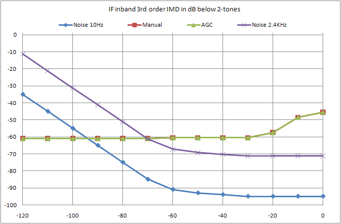
The following graph shows IMD measurement results of manual AGC and AGC in Attack/Decay mode. Also the noise floor measured in 10Hz and computed in 2.4KHz bandwidth is shown. The 2-tone separation is the standard 200Hz.
-
Manual
The red curve represents 3rd order IMD with Manual AGC. It uses a manual gain control setting such that the output level is identical to the situation with AGC enabled: typically -21dBm per tone at the output. This shows the IMD baseline that is built-in to the signal path when gain modulation due to a closed-loop is eliminated. Except for exceedingly strong input signals the built-in IMD is -61dBc for most of the gain control range.
-
AGC
The green curve represents AGC in Attack/Decay-Mode. It completely overlaps with the Manual AGC curve! Gain modulation does not add any significant IMD above the manual AGC baseline with the FAST/SLOW path AGC system described here. The IMD level is only -61dBc most of the gain control range. Maybe surprising too is that the SLOW path Attack and Decay settings do not influence the IMD level much. The observed IMD is the same for the slowest decay time possible: 6dB/s or 22s/131dB and for the fastest setting: 1546dB/s or 85ms/131dB and for any other decay speed in between these two extremes. So for "Very Slow", "Slow", "Medium", "Fast" and even "Very Fast" decay speeds, the IMD is still around -61dBc for most of the control range.
-
Noise 10Hz
The blue curve represents the noise floor measured in 10Hz bandwidth directly read from the spectrum analyzer. All IMD values shown below this noise floor have not been actually measured, but are copied from the first measurable value above the noise floor.
-
Noise 2.4KHz
The purple curve represents the noise floor scaled up to 2.4KHz bandwidth. (23.8dB added to the 10Hz values.) This curve approximately represents the signal to noise ratio in SSB bandwidth. The IMD exceeds the noise power in SSB bandwidth only from around S9 and upwards. The difference is not big and little can be done about it as it is AD600 built-in IMD.
The above graph only shows 3rd order IMD, which in analog systems is usually the strongest IMD component. Higher order IMD is quite important too as it sounds much worse. Therefore the next section shows spectrum analyzer pictures for S9, S9+40 and S9+60 signals with a span wide enough to also reveal 5th and 7th order IMD if there.
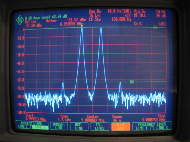
S9
The following picture shows the IMD plus 2-tones at the output of the Variable Gain Board with S9 (-73dBm) combined input level. The 3rd order IMD is -62dBc. 5th and 7th order IMD is below the noise floor.
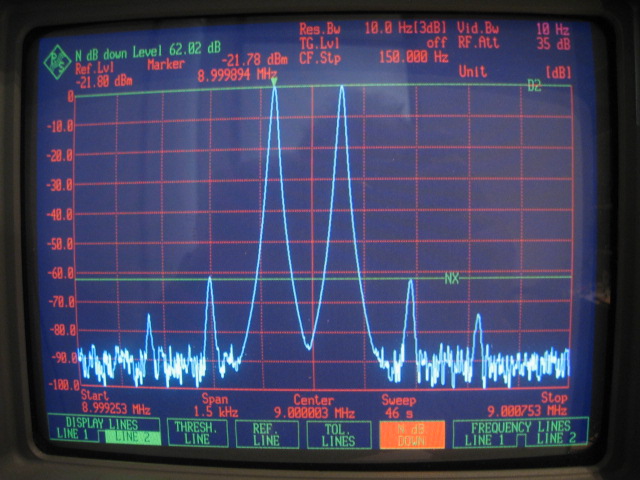
S9+40
The following picture shows the IMD plus 2-tones at the output of the Variable Gain Board with S9+40dB (-33dBm) combined input level. The 3rd order IMD is around -62dBc. 5th order IMD is around -74dBc. 7th order IMD is below the noise floor.
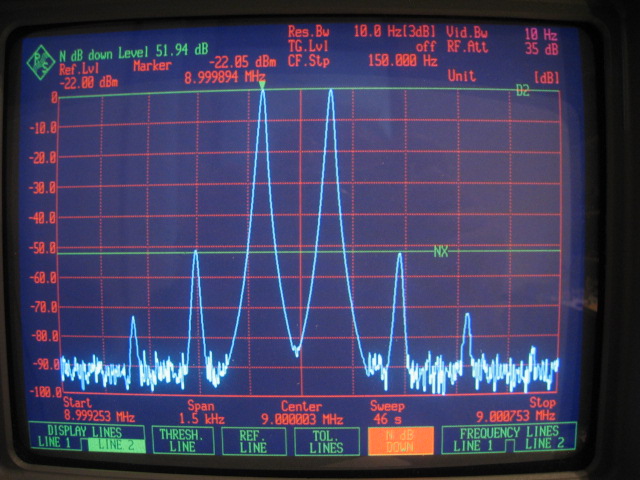
S9+60
The following picture shows the IMD plus 2-tones at the output of the Variable Gain Board with S9+60dB (-13dBm) combined input level. The 3rd order IMD is around -52dBc. 5th order IMD is around -72dBc. 7th order IMD is around -85dBc.
The previous three IMD pictures allow for good comparison with ARRL equipment reviews. The 2-tone separation of 200Hz and the S9 and S9+60dB levels have been chosen to accommodate this. More complicated is the characterization of "Fast AGC" and "Slow AGC" used by the ARRL. The exact definition of "Fast" and "Slow" can make all the difference in practice with some radios!
Conclusion
All gain modulation IMD results presented so far are with the AGC configured for Attack/Decay-Mode. This is the worst-case scenario, because the HANG phase represents temporarily an infinite decay time which helps reducing IMD and this phase is absent with Attack/Decay-Mode. However with this AGC system the results are the same with Hang-Mode and with Attack/Decay-Mode independent of SLOW path attack and decay times.
The AGC described here shows that it is possible for analog AGC to rival digital AGC with respect to gain modulation IMD and fast attack with continuous linear operation of the signal path.
In fact the principle of gain modulation IMD applies equally to AGC implemented in the digital domain with DSP as it does to analog AGC. If a VGA chip is used in front of the ADC to increase its dynamic range, then the DSP solution can become quite challenging because of the severe time delay of a brick wall digital filter now inside the feedback loop! This is exactly the problem that is prevented on the Variable Gain Board by eliminating the narrow crystal filter inside the loop.
The goal to keep the in-channel IMD below -60dBc in the signal path has been met also in the face of gain modulation IMD for most of the AGC's control range. The next challenge will be to not spoil this result with either the product detector or the audio circuits that complete the signal chain!
Please follow the links below to read more about the other aspects of the Variable Gain Board.
Signal Path
Control Path
Closing the Loop
Set-point Reference
Back to Variable Gain Board
Back to the TOC
|