Block Diagram
The ultimate selectivity of the receiver has to be established before any significant gain is applied in the signal path to keep the in-band as well as out of band IMD as low as possible. The selectivity board is designed to provide the ultimate receiver selectivity behind the frontend roofing filters at the expense of only a minor increase of the cumulative NF of the receiver. The block diagram of the selectivity board following the frontend board in the signal path is shown in the picture below:
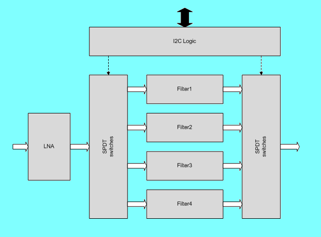
The design of this board is very straight forward. The 9 MHz frontend signal enters the diagram at the left. This point has the lowest signal level inside the signal path as no gain has been applied yet. The accumulative losses of antenna filter, H-Mode mixer and roofing filter directly set the base line for the noise figure of the receiver. So at this point a low noise amplifier is needed to prevent further degradation of the receivers NF with the additional insertion loss of the selected quality quartz filter. The LNA should have a very low NF, combined with moderate gain and good IMD3 performance. Not enough gain and / or too high NF will hurt the cumulative NF of the receiver. Too much gain and / or bad IP3 will hurt the in-band IMD performance. Basically the LNA should generously compensate the loss of the quartz filter without introducing much IMD or noise itself.
The bank of SPDT switches on both sides of the 4 available filter slots will select the desired quartz filter by means of I2C control. A 2.4KHz SSB filter together with a 500Hz CW filter are probably the minimum for a general purpose amateur bands receiver. The 2 reserve filter slots could be used for a narrower "contest" 1.8KHz SSB filter and a 250Hz CW filter. Wider filters than the frontend roofing filter make not much sense.
Assembly
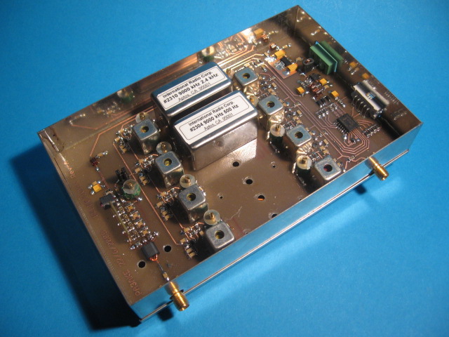
The selectivity board assembly in its tin metal box is depicted in the photo below:
The module is euro-card sized and follows the general layout rules used consistently in this project:
-
Power and I2C control connector are located at standard positions at the right edge of the board.
-
SMA connectors are located at the bottom edge of the board and provide the signal interface to the board.
The board contains the following sub-circuits, which can easily be recognized from the picture:
-
Low noise pre-amplifier to compensate for the losses introduced by the filters.
-
4 pairs of SPDT bus switches to select 1 of in total 4 quartz filters.
-
In total 4 quartz filters with low pass L-matches. Two filters are actually installed on the picture.
-
I2C hardware to control the filter selection through I2C with a microcontroller.
-
On-board LDO regulators and extra power supply filtering.
Separate pairs of L-matches per filter are used in order to get the best match possible for each individual filter. In theory just 1 set of L-matches would suffice if all installed filters have identical design impedance (usually 500Ω at 9 MHz). But in practice this would be sub optimal as filters are never identical, certainly not when they have different design bandwidth! Furthermore it is much better to switch the filters in a 50Ω system rather than a 500Ω system as small parasitic L's and C's in the layout will play a far lesser role. With bus switches (MOSFET's) the 50Ω choice is a must to keep the signal voltage within Vdd and Vss and to keep IMD low given the high dynamic range at this point in the signal path. In order to be able to squeeze out the best match that is possible, all L-matches have both their L and C part adjustable. This is important as only slight mismatches with only little extra ripple in the frequency domain insertion loss plot have far bigger effect on the group-delay peaks at the filter edges. Group-delay peaks are signs of phase distortion and should be minimized as much as possible.
The board has room for 4 crystal filters and the 9 MHz quartz filters distributed by INRAD are supported. The picture shows the #2310, 2400Hz wide for SSB and the #2304, 500Hz wide for CW. When the white stickers are removed, the printing on the metal can done by the actual manufacturer is revealed, and it looks like these filters are manufactured in Japan. The INRAD filters are cost effective and of reasonable quality. There does not appear to be a 9 MHz 250 Hz CW available at INRAD. If there was one, it remains to be seen how well it would work especially with ringing. In practice a more selective but far more ringing filter does not allow you to copy a weak CW signal better, on the contrary!
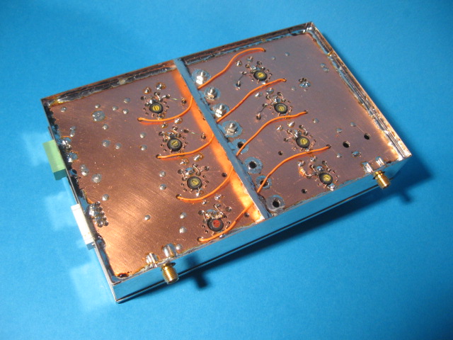
The next picture shows the back side of the assembly with the lid removed. The orange wires carry the DC voltage to control the SPDT switch pairs. These wires are intentionally not part of the PCB layout in order to not disturb the ground-plane of the board. For this early prototype the bottom plane has not been etched anyway and the through hole L45-6 coil former and crystal filter connections have been "ugly-wired" as well. A metal shield that firmly connects with the bottom lid to prevent any leakage on this side of the board is also visible.
Apart from INRAD filters, it is also possible to install filters manufactured by KVG, such as the well known XF9B. KVG filters are a bit wider physically, so only 3 will fit together. I hope to do some comparative tests with KVG filters in the future!
Adjustment
The only "analog" adjustment needed to commission the Selectivity Board is to properly match the installed crystal filters with their associated L-matches. A VNA is best used to accomplish this.
Solder jumpers SJ1, SJ2 and SJ3 determine the I2C address of IC9. They should be configured such that there are no conflicts on the I2C bus with the addresses of other I2C chips.
Solder jumpers SJ4 and SJ5, which enable I2C-bus terminating resistors R16 and R17 should only be soldered in if the Selectivity Board is positioned at the end of the physical I2C-bus.
Documentation
The following link points to the Selectivity Board documentation file available for download for those who wish to reproduce the unit:
Selectivity Board documentation in PDF format
This PDF contains:
-
Schematics.
-
Bill of materials.
-
Component side, scale 1.6.
-
Back side, scale 1.6, showing the 4 tracks to be wired by hand.
-
Top side, mirrored scale 1, for PCB production.
-
Bottom side, mirrored scale 1, for PCB production if needed.
Specification
The following table summarizes the key parameters of the selectivity board:
| Selectivity Board Specs |
| Dimensions |
160 x 100 x 30 |
mm |
| Weight |
380 |
gr |
| Supply Voltage |
+13.5 to +15 |
V |
| Supply Current |
130 |
mA |
| Input Impedance |
50 |
Ω |
| Output Impedance |
50 |
Ω |
| Noise Figure |
1.3 |
dB |
| Input Return Loss at 9MHz |
< -20 |
dB |
| Reverse Isolation at 9MHz |
< -40 |
dB |
| Pass Through Filter |
| Gain |
11.3 |
dB |
| IMD |
< -70 |
dBc |
| IIP3 |
+23 |
dBm |
| Pass band Ripple |
0 |
dB |
| Stop band attenuation |
0 |
dB |
| #2310 SSB Filter |
| Gain |
9.0 |
dB |
| IMD, input level < -2dBm |
< -65 |
dBc |
| IMD, input level < -18dBm |
< -71 |
dBc |
| Out-of-band IIP3 |
+23 |
dBm |
| Pass band Ripple |
0.15 |
dB |
| Stop band attenuation |
90 |
dB |
| #2304 CW Filter |
| Gain |
5.1 |
dB |
| IMD, input level < -10dBm |
< -50 |
dBc |
| IMD, input level < -32dBm |
< -62 |
dBc |
| Out-of-band IIP3 |
+23 |
dBm |
| Pass band Ripple |
NA |
dB |
| Stop band attenuation |
85 |
dB |
Please use the following links to navigate to the detailed discussions of the following subsystems:
Filters
Switches
Pre-Amplifier
Back to IF Introduction
Back to the TOC
|