AD9910 versus AD9912
Both AD9910 and AD9912 are promising candidates for the implementation of an HF LO with a pure DDS with their 1GHz clock capability and 14-bit DAC. In general they have similar specifications when it comes to key areas like SFDR and phase noise. My guess is that they share identical subsystems like the DAC for instance. Apart from that, there are many differences, because the chips are meant for different applications.
The AD9910 allows for full control of phase, amplitude and frequency with its 16-bit POW (Phase Offset Word), 14-bit ASF (Amplitude Scaling Factor) and 32-bit FTW (Frequency Tuning Word) registers, combined with support for more complex modulation schemes with a high speed parallel port. The AD9912 on the other hand does not support detailed amplitude control, but has a 48-bit FTW and with its different output squarers, dividers and multipliers seems to be aiming at the programmable clock oscillator market!
My first preference goes to the AD9910 because some of its features are more useful as a building block in an HF transceiver. Worth mentioning is the hardware support for multi-chip synchronization, which is great for creating quadrature signals needed for image rejecting mixers, and also OSK (Output Shift Keying) that allows for detailed programming of the envelope of a keyed signal, which is useful for CW transmitting.
The AD9912's advanced features, such as the "Spur Killer Technology" seem less useful for the HF-LO. The output frequency is very low relative to the Nyquist limit and Spur Killer does not add much in that scenario. Also the different output squarers/multipliers/divider options seem less useful. The extra frequency resolution of up to 4μHz possible with the 48-bit FTW is not really essential too.
Therefore the AD9910 was chosen as the first chip to evaluate for its performance in the HF-LO DDS application.
AD9910 prototype board
Encouraged by the arrival of pre-production samples of the AD9910 and the promising spur and phase noise pictures in the pre-release datasheet, a PCB layout was designed that could be homebrew cooked in the "kitchen", to put those samples to the test. I knew that the large TQFP100 0.5mm pitch package was going to be at the very limits of what is possible with the PNP-blue technique for PCB's. Especially the thermal pad underneath gives extra complications as it needs to be soldered to the ground plane. This really asks for a PCB with plated-through holes. Still I wanted to prove that it is possible to completely homebrew such a board. This first design was made with the following features to help promote low spurs and phase noise as much as possible:
-
Separate analog and digital ground planes are used to minimize spurs.
-
Power supply partitioning with 4 separate regulators in order to minimize spurs.
-
A double sided layout is used, where the bottom plane is almost completely devoted to the ground planes.
-
The reference clock input circuit feeds the AD9910 symmetrically with a balun.
-
The DAC output circuit uses a well balanced wideband 1:1 transformer.
-
The anti-alias filter is an 11th order elliptical design with a 100MHz cut-off frequency.
-
Support for multi-chip synchronization is possible with an optional header connector.
Support for the high speed parallel port was omitted. The usage of that port is not anticipated in the HF-LO DDS application and furthermore the associated layout would simply be too complicated for a 2-layer homebrew board. The following picture shows the resulting fully assembled and functional prototype assembly:
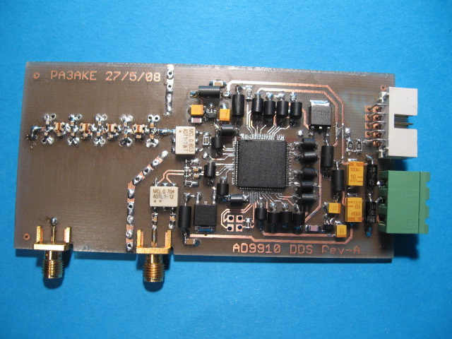
The board size is 110x55mm. Old "Junk-box" through hole ferrite beads are used to get the 1.8V and 3.3V from the 4 regulators to the individual pins of the chip. Most decoupling chip capacitors are on the bottom side of the PCB. It turned out to be a really difficult job to get this PCB assembled. The lack of a solder resist layer did not help in cleanly soldering the 100 pins and getting the thermal pad connected to the ground plane was a real struggle...
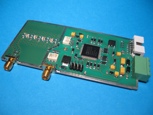
Initially I could not get this board to work, so after many attempts I was more or less convinced that I had somehow fried the chip thermally or otherwise killed it through ESD. I reworked the PCB to be produced commercially using smaller parts with more and smaller VIA's and that board proved to be much easier to assemble. The following picture shows the second AD9910 prototype board attempt:
However, much to my surprise and dismay, this new board also did not work initially. In the end it turned out not to be an electrical problem with both boards, but completely a software problem! I had naively programmed the AD9910's registers as if it were similar to the AD9951. So I programmed its FTW register directly. This does not work like with the AD9951. Instead, 1 of the 8 possible single tone profiles register sets should be used in order to get a single tone from this chip. The explicit FTW register in the register map of the AD9910 is used only in the more advanced modulation schemes and is ignored / overruled in single tone mode... How about reading the "!@#" manual first?
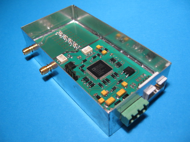
The main result from this exercise is that, although it is possible to completely homebrew boards holding 100 pin 0.5mm pitch parts, it is rather troublesome, especially due to the pad underneath these chips. A much higher chance of success is possible with a professionally made double sided board with plated-through holes. To complete the slide show of the second prototype, the following picture shows the board when soldered into a metal enclosure:
AD9910 Spurs
Initial tests of the 2nd prototype board, when used as a LO in my experimental HF receiver, showed that the spurs produced by the AD9910 are very weak indeed. Significantly better than with its predecessor, the AD9951. It really is an order of magnitude better. Although the comparison with the AD9951 is not completely fair as the AD9951 board I compare against (I0CG) has a 200MHz anti alias filter rather than a 100MHz filter, no separation of analog and digital ground planes and no separate regulators for analog and digital power supplies, which will not be helpful in fighting the spurs.
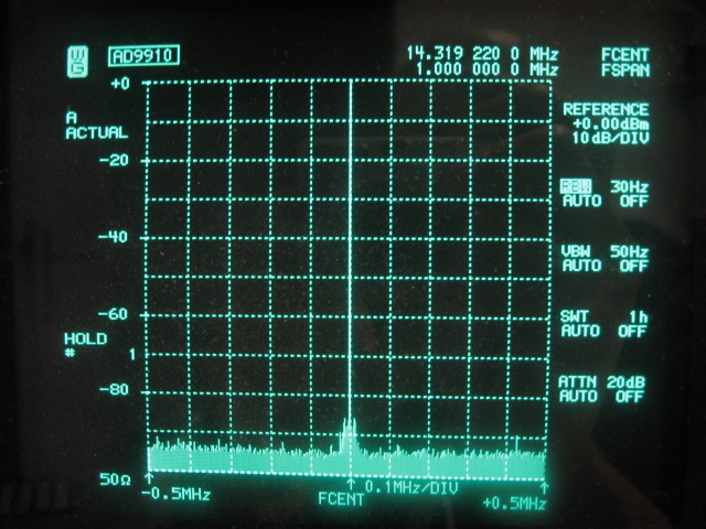
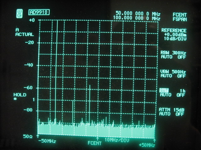
I0CG's AD9951 board, when used as a LO in my experimental receiver, produced 130 audible spurs, when tuning the receiver on 15M band between 21.000MHz and 21.450MHz. These spurs are documented here, although not with the more spurry but IP3-wise better T1-6T transformer mixer configuration. Many spurs are at or below MDS level, however a couple of spurs are quite strong. With the AD9910 board, all spurs but 4 disappear completely. With 'disappear' I not only mean that they are below MDS and in the noise, they are so far below MDS that they cannot be heard anymore in SSB bandwidth. The persisting 4 spurs are around or slightly below MDS level. This is a very significant improvement, which makes the extra complexity needed to clock the chip at 1GHz absolutely worthwhile. The following plot shows a virtually spur free 1MHz wide view of a 14.3MHz 0dBm DDS output signal. Note that the noise floor is introduced by the analyzer and so is the little blob of noise at the bottom of the carrier.
The next picture shows the complete 100MHz spectrum that is passed un-attenuated by the anti alias filter. The worst spurs are close to 90dB below the carrier and the 2nd and 3rd harmonics of the output signal are already very weak, which also tells something about the accuracy achieved with the 14-bit DAC of this DDS chip.
In fact, most of the spurs with the AD9910 at these low output frequencies with respect to Nyquist, are so far below the carrier that they cannot be properly observed within the dynamic range of my spectrum analyzer. They will become easily visible however when the DDS signal is inspected with a phase noise test set designed to expand beyond the normal dynamic range of the spectrum analyzer.
Anti alias filter
The excellent spur (category 3) results with the AD9910 used as the LO of the receiver are at least partially explained by the 11th order 100MHz anti-alias filter. It is an elliptical low pass filter with a theoretical stop-band of -90dB. The filter layout is made with the recommendations presented in application note AN-837 in mind. This paper by David Brandon of Analog Devices, shows how much deterioration of the filter stop band can be 'achieved' with small and crowded layouts. Therefore I have devoted a lot of space and VIA's to the anti alias filter on the prototype board. The following picture shows the first 500MHz of the filters transmission plot:
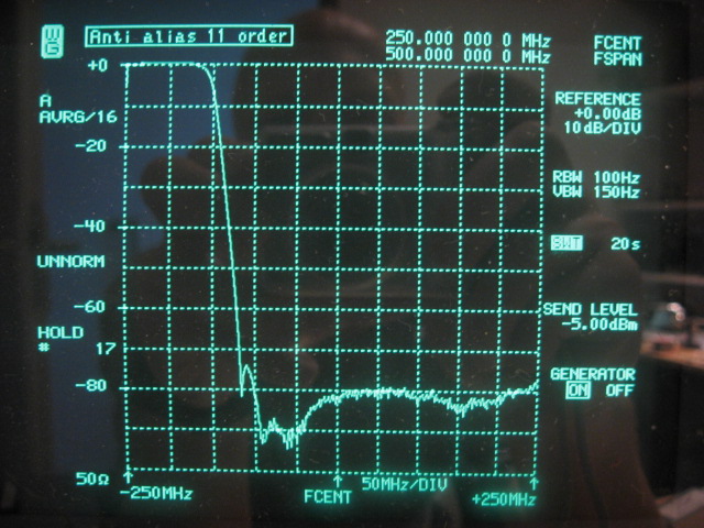
The LPF behaves close to what was simulated, at least in this part of the spectrum, except that the stop band is a little less at -80dB rather than the designed and simulated -90dB. The following picture shows the behavior over a much wider frequency range, revealing some 'issues' that demonstrate how theoretical and less meaningful circuit simulations can be if parasitic effects are not also taken into account:
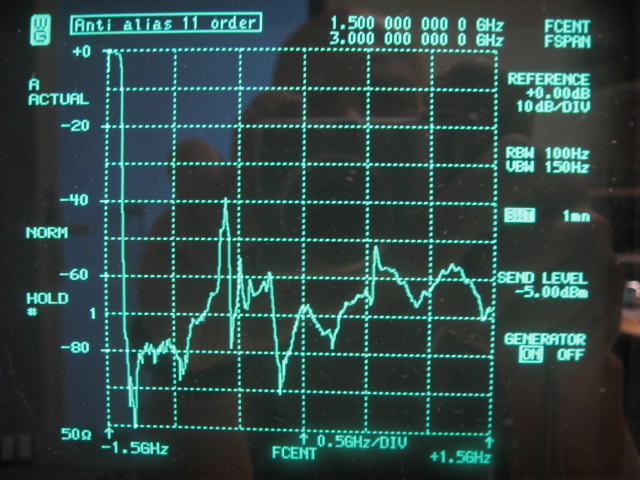
The biggest issue is the stop-band deterioration to as worse as even -40dB around 1GHz, right where we need good stop-band so much! ATC-100A microwave chip capacitors have been used with self resonant frequencies that are way beyond 3GHz, so the capacitors self inductance is not the problem. The SMD coils however are self resonant around 1GHz. To solve this issue a small 'monolithic' SMD low pass filter has been added with a 400Mhz cut off frequency to help the discrete elliptical filter at frequencies where its inductors are misbehaving. The SMD filter has much less ultimate stop band performance, but it is capable of maintaining those specs up to at least 3GHz. The results are shown in the following picture:
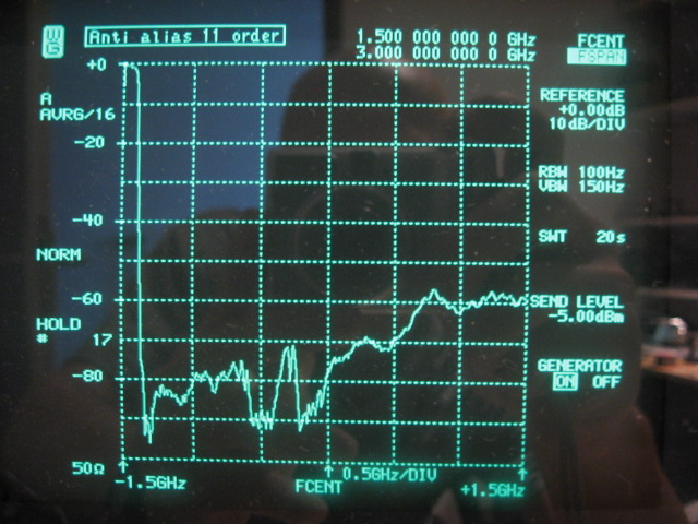
The stop band around 1GHz is much improved even to -90dB, but above 1.5Ghz the improvement is not what we hoped for. In the next version of the board it will be determined if extra shielding with compartments can further improve things. It is unclear at this moment if "blow-by" or "blow-through" is occurring beyond 1.5GHz. To be continued!
The following picture shows the resulting output of the DDS board running at a 14.3MHz output frequency with the improved anti-alias filter over the frequency range (> 100MHz) that the filter is supposed to block:
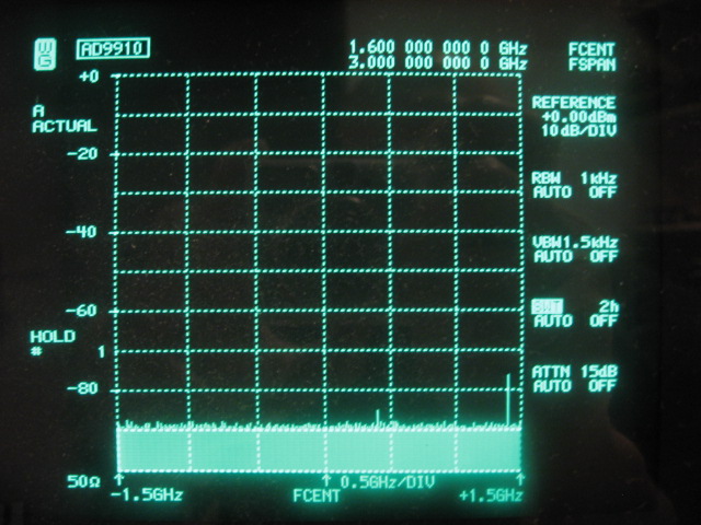
Although the filter does not maintain its stop-band very well above 1.5GHz, the -60dB it gives around 3GHz proves to be adequate. The resulting spectrum is remarkably clean. The 2nd and 3rd harmonic of the reference clock are the only visible spurs at -85dBc and -76dBc respectively. All other spurs are down by at least 90dB's!
1GHz Reference Clock
AD9910 Prototype Board
AD9910 and SSB-Noise
AD9910 and PM-Noise
Back to Design Choices
Back to the TOC
|