Mother Board
After many experiments, especially on 40M, to produce band pass filters with sufficiently high IP3 and low insertion loss the end conclusion was that the BPF subsystem was not likely going to be very small. The rather big T94 toroids would take up a lot of space and made a single PCB not practical.
Therefore the motherboard approach was chosen as it allows for a more compact 3D solution giving plenty of space for each individual filter board. Also the flexibility by exchanging filters and even spare slots is attractive. On the down side it is a lot more work from a constructional point of view and extra complications with for instance the connectors may show up.
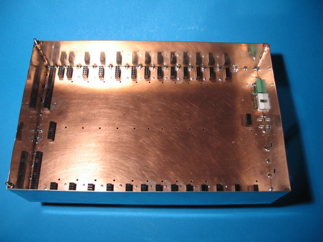
The following picture shows the component side of the motherboard. The only components are connectors. It basically forms a huge ground plane. Up to 12 BPF boards can be inserted in this version. There are also slots for a notch filter board, an attenuator board and the I2C control board. The size is 25cm x 16cm.

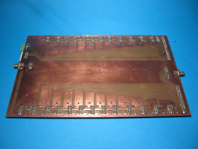
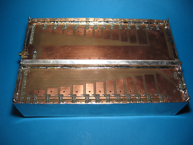
The following picture shows the bottom side of motherboard. It provides all the tracks to distribute the RF-signal and the relay control lines to the individual sub-assemblies. Difficult to see on the picture are the many 0805 100n decoupling capacitors on the relay control lines close to the connectors. Those lines are also kept strictly separate between the 2 sides in order to minimize signal leaks bypassing the filters and worsening the stop band performance.
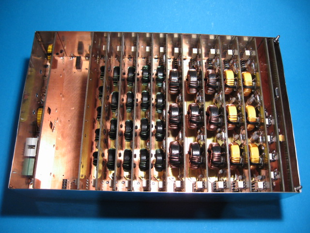
Next is a picture with all the boards inserted. The board in front is the 9MHz notch filter, followed by 2 spare slots and then the 10 BPF's, beginning with 6M.
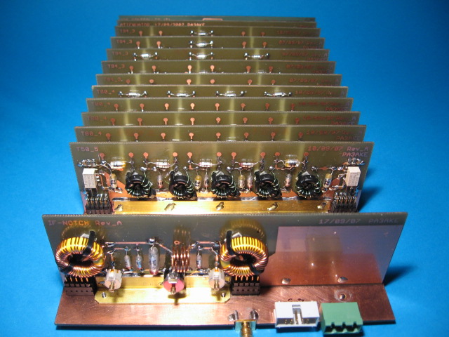
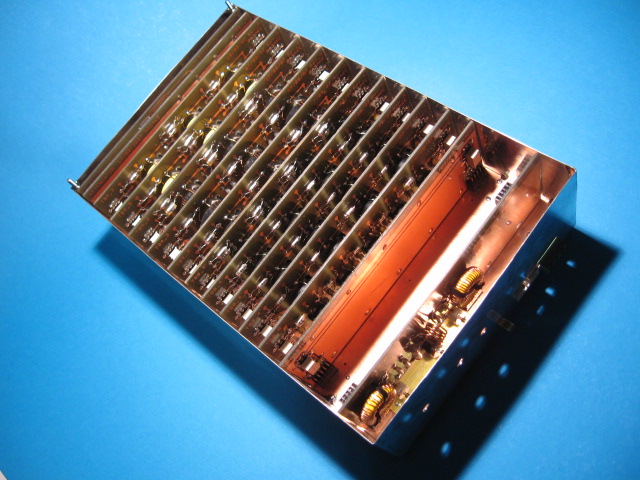
From left to right: The I2C controller board, the attenuator board, 10 BPF boards, 2 spares and the IF notch filter board. From this side it can be seen that the 160M through 20M boards have more space to allow for the bigger T94 toroids.
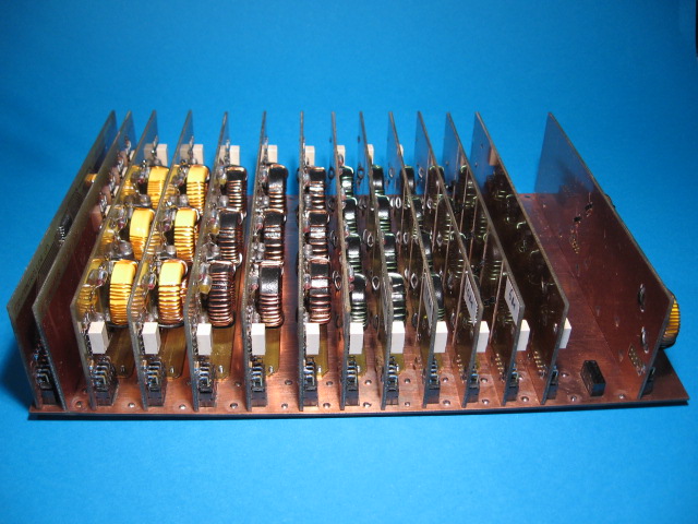
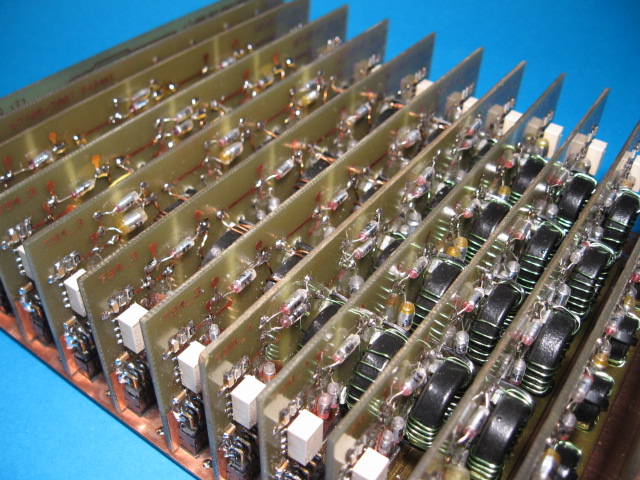
From the top it looks rather cramped but the individual filters have enough "air" to breath. The end result is a rather compact solution that allows for good stop band performance where the individual filters cannot "see" each other. The filter boards have ground planes that effectively shield the boards from each other.
The following picture shows the empty mother board with the surrounding metal work completed.
In order to get the best stop band performance the bottom compartment has been divided in two. This primarily improves stop band in the VHF region.
Top view again with all the boards mounted. The notch filter board is to the left and 3 holes allow access to the trimmers to do the final adjustments with the box closed.
From a different angle...
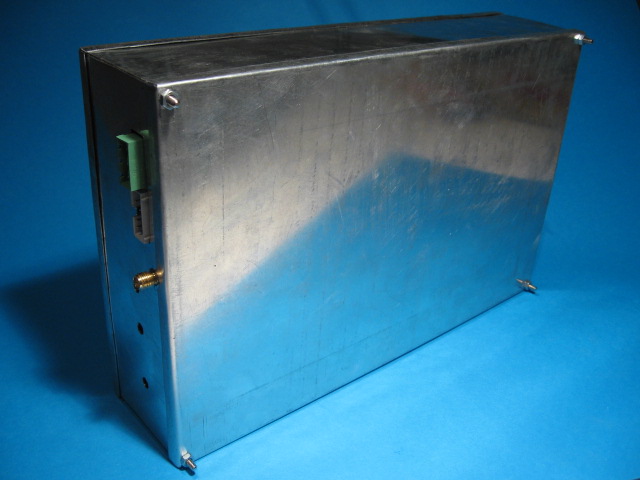
And finally completely inside its enclosure. Now it is just a big metal box measuring 25cm x 16cm x 6cm with power, I2C and SMA connectors.
Constructional issues
Due to its size, fabricating the PCB "at home" becomes a bit of a challenge. First of all the artwork must be transferred to the board. I have used the PnP-Blue method with good enough result in the end, but not without complications.
Due to heating up of the foil by the laser printer, the foil came out just a little bit larger than printing the same thing to paper! The error had to be corrected because absolute accuracy is needed for the plug-in boards to be plugged in!
Next, many laser printers have inaccuracies that are usually not noticeable with smaller layouts without connectors on both ends. The printer I use is correct on the X-axis but has a noticeable scaling error on the Y-axis... Luckily the absolute accuracy of the Y-axis is not important with this design.
Also transferring the "blue" to the copper gave inaccuracies. Although very little pressure was used, still the result was slightly uneven deformed, but within tolerances. Initially I wanted to etch the top side (just square holes for the connectors) also with the PnP-blue method. This did not succeed at all. The deformation after ironing was too difficult to contain and I ended up by simply taping the top side and cutting out the connector areas.
It is probably best to produce this PCB the photographic way. When the foil is professionally plotted rather than laser-printed, to avoid heating up problems, the results will be very good.
PCB artwork for the BPF motherboard in PDF format.
Note the two 4K7 "wetting current" resistors and the two 100n capacitors on the bottom layer. Furthermore, each relay control line is decoupled to ground as close as possible to the connector with a small 0805 100n capacitor. They are not visible on the artwork but should be mounted too!
I2C Controller Board
Attenuator Board
Band Pass Filter Board(s)
IF Notch Board
Back to Frondend Input Band Pass Filters
Back to the TOC
|