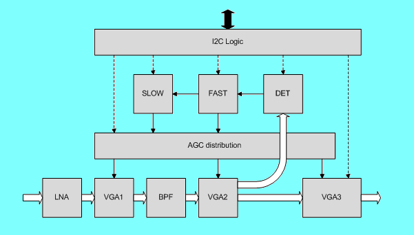
Block Diagram
The board that follows the Selectivity Board in the signal path is the Variable Gain Board. The selectivity board sets the ultimate selectivity of the receiver. Now it is time to raise the signal level substantially and to apply manual and / or automatic gain control (AGC), which is the purpose of the Variable Gain Board. The block diagram is shown in the picture below:
The 9 MHz IF signal enters the diagram at the left. This point still has a very low signal level. Only 12dB gain has been applied versus 10.5dB combined losses in case of the #2310 SSB filter and 15.8dB combined losses in case of the #2304 CW filter.
SSB frontend gain = -1.5 (BPF) - 5.0 (mixer) - 1.0 (ssb-roofer) + 12.0 (LNA) - 3.0 (ssb-filter) = +1.5dB
CW frontend gain = -1.5 (BPF) - 5.0 (mixer) - 2.4 (cw-roofer) + 12.0 (LNA) - 6.9 (cw-filter) = -3.8dB
A preamplifier (LNA) with very low noise figure is needed to not degrade the cumulative noise figure of the receiver. The signal path is build around the AD600 VGA by Analog Devices. The first two VGA stages are inside the AGC feedback loop. The third stage is using feed-forward to exactly keep the output level constant over a very wide input signal range. There is only 1 detector that drives a slow and a fast AGC feedback path.
The block diagram and the AD600 VGA component choice shows similarity with the well known IF strip published by Bill Carver, W7AAZ. The article, 'A High-Performance AGC/IF Subsystem', was published in QST, May 1996. Bill's high end IF has been popular since then and it is reproduced by many CDG2000 builders. The variable gain board presented here should be seen as a natural evolution of this design. Without that starting point there would not have been a Variable Gain Board as it is now! Reading Bill's original article will give helpful background information to better understand the design presented here.
The top level differences with regard to the original are:
-
One detector + AGC loop with fast and slow path, rather than two detectors with fast loop and slow loop.
-
A very flexible AGC strategy capable of providing both Hang-Mode and Attack/Decay-Mode AGC.
-
Complete control of user and system set-points through I2C. Only 1 trim pot-meter remains.
The precise "why" and the "how" of the above points will be discussed in more detail deeper down the hierarchy of this web-document.
Assembly
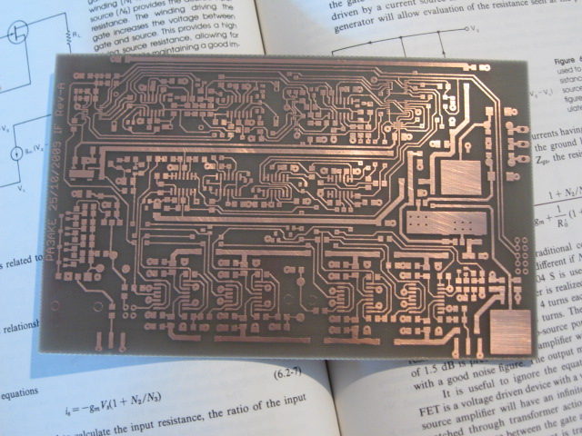
In total two prototype builds have been necessary to arrive at the current Variable Gain Board version B. Prototype 1 needed in total 3 modifications that improved the IMD behavior to the level described in this web document. The following picture shows the component side of the "kitchen cooked" prototype 1 PCB:
Variable Gain Board prototype 2, fully assembled in its tin metal box, is depicted in the photo below. Note the change in color around the three LDO regulators mid right in the picture. This area has become hot enough to cause a slight change in color of the clear lacquer protecting the PCB surface. This is due to too much combined dissipation of the voltage regulators concentrated in that area. The regulators actually never entered thermal overload protection even during many hours of continuous operation during the hot 2010 European summer. This thermal issue has been solved now with the introduction of a precise pre-regulated switched-mode +14V and -14V dual supply voltage.
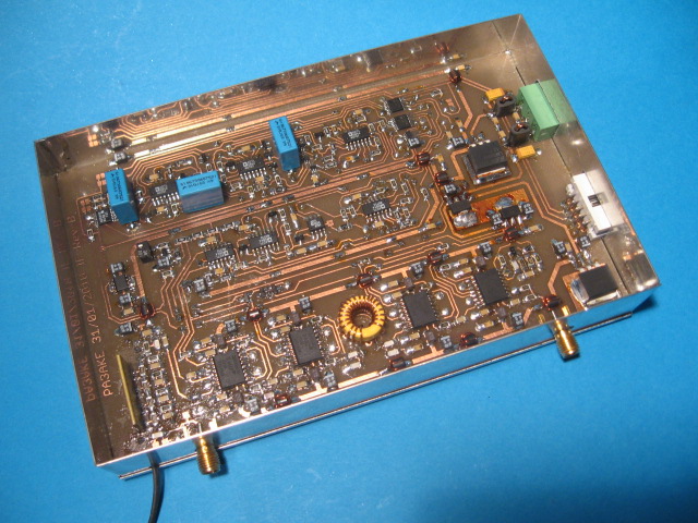
The module is euro-card sized and follows the general layout rules used consistently in this project:
-
Power and I2C control connector are located at standard positions at the right edge of the board.
-
SMA connectors are located at the bottom edge of the board and provide the signal interface to the board.
The board contains the following sub-circuits, which can be recognized from the picture:
-
Quad JFET low noise pre-amplifier.
-
A chain of 4 AD600 dual-VGA chips.
-
The several ADTL084 quad-OPAMP's that implement the AGC behavior.
-
I2C hardware to control the board through I2C with a microcontroller.
-
On-board LDO regulators and extra power supply filtering.
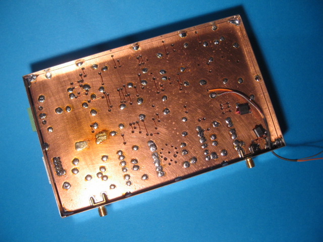
The other side of the unit is shown below. This prototype uses a full ground plane where a number of short vertical tracks are not etched in the layout, but simply manually wired. It is also possible to mount the wire bridges at the top side of the board. The two small transformers of the Quad JFET LNA however have to be mounted at the bottom side of the board.
Adjustment
Three simple adjustments are needed for proper operation of the Variable Gain Board:
-
The reference voltage must be set with R88 and an accurate digital multi-meter. See: Reference.
-
The noise filter must be centered with L1 at 9MHz. See: Noise Filter.
-
The end of the gain control range must be set. See: Vfloor.
Solder jumpers SJ1, SJ2 and SJ5 determine the I2C addresses of IC16, IC18 and IC19. They should be configured such that there are no conflicts on the I2C bus with the addresses of other I2C chips.
Solder jumpers SJ3 and SJ4, which enable I2C-bus terminating resistors R41 and R42 should only be soldered in if the Variable Gain Board is positioned at the end of the physical I2C-bus.
Documentation
The following link points to the Variable Gain Board documentation file available for download for those who wish to reproduce the unit:
Variable Gain Board documentation in PDF format
This PDF contains:
-
Schematics.
-
Bill of materials.
-
Component side, scale 1.6.
-
Back side, scale 1.6, showing the tracks to be wired by hand.
-
Top side, mirrored scale 1, for PCB production.
-
Bottom side, mirrored scale 1, for PCB production if needed.
Specification
The following table summarizes the key parameters of the variable gain board:
| Variable Gain Board Specs |
| Dimensions |
160 x 100 x 30 |
mm |
| Weight |
290 |
gr. |
| Positive Supply Voltage |
+13.5 to +15 |
V |
| Positive Supply Current |
250 |
mA |
| Negative Supply Voltage |
-13.5 to -15 |
V |
| Negative Supply Current |
140 |
mA |
| Input Impedance |
50 |
Ω |
| Output Impedance |
50 |
Ω |
| Noise Figure |
2.15 |
dB |
| MDS measured in 2.4KHz bandwidth |
-138 |
dBm |
| Maximum allowable input signal |
+3 |
dBm |
| AGC Threshold |
-115 |
dBm |
| Output Level above AGC threshold |
-17 |
dBm |
| -3dB Bandwidth |
212 |
KHz |
| Center Frequency |
9 |
MHz |
| S/N ratio for -70dBm, (S9+3) |
60 |
dB |
| S/N ratio ceiling for > -40dBm, (S9+33) |
70 |
dB |
| Minimum Gain |
-21.5 |
dB |
| Maximum Gain |
109.6 |
dB |
| Gain range, open-loop |
131 |
dB |
| Gain range, closed-loop |
121 |
dB |
| IMD, input level < -30dBm, (S9+43) |
-60 |
dBc |
| IMD, input level < 0dBm, (S9+73) |
-45 |
dBc |
| AGC: Attack/Decay-Mode |
Yes |
|
| AGC: Hang-Mode |
Yes |
|
| AGC: Manual-Mode |
Yes |
|
| AGC: I2C controlled |
Yes |
|
| Attack Time |
1 |
ms |
| Maximum Decay Speed |
1550 |
dB/s |
| Minimum Decay Speed |
6 |
dB/s |
| Maximum Hang Time |
30 |
s |
| Minimum Hang Time |
120 |
ms |
| S-meter accuracy above AGC threshold (8-bits) |
1 |
dB |
| Output flatness above -90dBm |
1 |
dB |
Please use the following links to navigate to the detailed discussions of the following subsystems:
Signal Path
Control Path
Closing the Loop
Set-point Reference
Back to IF Introduction
Back to the TOC
|