Introduction
Like the other maybe more challenging subsystems in the receiver project, the audio subsystem will also be treated as a first class citizen in the signal path. The typical application of a low power integrated amplifier, together with a small internal speaker, will unnecessarily add at least some distortion and this can quite easily be improved upon. The audio subsystem can be made to perform such that it will not be a weak link in the signal path and integrates well in a modern PC-equipped shack.
Block Diagram
The board that follows the Detector Board in the signal path is the Audio Board. This board is the final board in the signal path. It distributes and amplifies the audio IQ output signal from the Detector Board to a power level suitable for speakers / headsets / line-out. The block diagram is shown in the picture below:
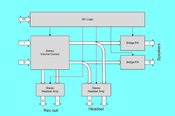
The design of the Audio Board is straight forward. It is more or less an "application-note" type of easy going circuit and most of the details can be found in the datasheets of the IC's being used. Nevertheless a brief walk-through of the circuits is given.
The IQ audio signal enters the block diagram at the left. It is first processed with a TDA7309 audio processor. This analog audio chip is fully I2C controlled, has nominally 0dB gain and takes care of the following functions:
-
Input signal selection. The circuit is wired to provide the following choices with its 4 position stereo input multiplexer: IQ-Off, II-Mono, QQ-Mono, IQ-Stereo.
-
Volume Control. It provides independent volume control for both channels over a 95dB control range in 1dB steps. Obviously volume and balance control can be directly implemented with this. But also a compensation for difference in audio volume between different modes such as SSB and CW is possible.
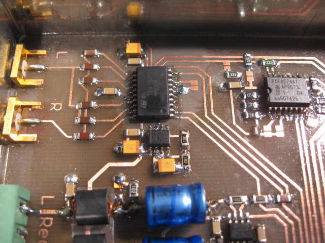
The picture below shows the TDA7309 and I2C section of the Audio Board in close-up.
The TDA7309 is followed by 3 sets of stereo amplifiers with the following purposes:
-
TS486 stereo headset amplifier used to provide line-out IQ signal independent of the volume setting. Its gain is fixed at 0dB. This output signal pair is suited to connect with a PC's soundcard to provide further digital signal processing. Apart from the obvious application to decode digital communication modes or Morse, other possible use is noise reduction, notch filtering or simply audio recording.
-
TS486 stereo headset amplifier to drive a headset. The gain is fixed at 20dB, which should be loud enough for most headsets.
-
A pair of TDA7391 32W power amplifiers to drive the speakers. TDA7391 is a class AB bridge amplifier intended for the automotive world. At the typical output power used in this radio application its distortion is very low.
The following picture shows the 3 stereo amplifiers on the Audio Board in close-up. Note that ferrites at the outputs have been used to block RF that possibly could be picked up during transmissions.
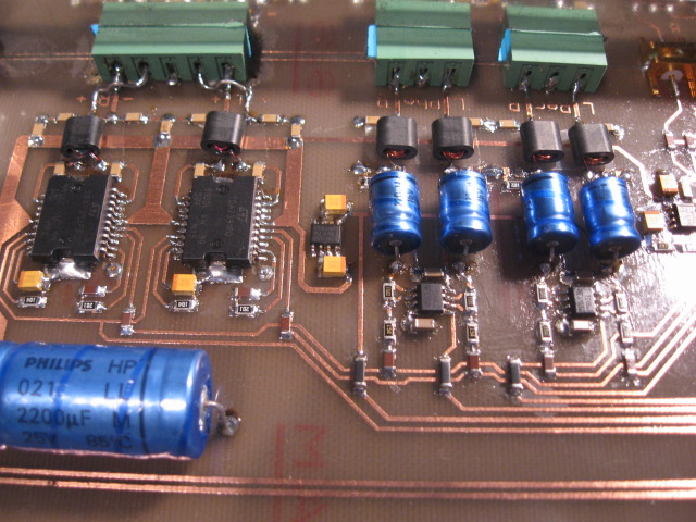
The two TDA7391 power amplifiers on the left are soldered with their thermal pad to the ground-plane of the board. Twelve VIA's per amplifier are used to transfer the heat to the copper ground-plane. Additional heat sinking will be needed if these amplifiers are actually used at their rated power output! The Rev_B layout has holes in the PCB to help with mounting heat sinks. The picture shows the first prototype Rev_A layout on which accidentally the wrong connector package was routed for the speaker outputs...
From the block diagram and the schematic it can be seen that each stereo amplifier can be individually enabled/disabled through I2C control.
Distortion
Discussion of the Audio Board is not complete without an attempt to assess the distortion that it introduces in the signal path. No low frequency signal generators of sufficient quality are available here to actually provide the test signals to do this measurement. Instead, two RF signal generators at 9MHz are used together with the Detector Board to produce the 1-tone and 2-tone test signals for the Audio Board. The Detector Board produces IMD < -80dBc with respect to the 2-tones with a combined level of -17dBm, with the SSB filter noise selected. The tests should now provide evidence that the Audio Board adds no noticeable additional distortion.
The first test is a standard 2-tone test with 200Hz separated tones. The following picture shows the output spectrum of the line-out amplifier over a 3KHz wide span from 86Hz to 3086Hz:
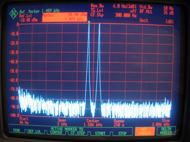
The IMD level is below the 6Hz RBW noise floor. The only visible sign of distortion is not IMD, but harmonic distortion. A spur of -77dBc at 2.978KHz is visible. This is the 2nd harmonic of the left input tone. This calls for a 1-tone test to further inspect harmonic distortion. The following picture shows the response to a single tone at 482Hz.
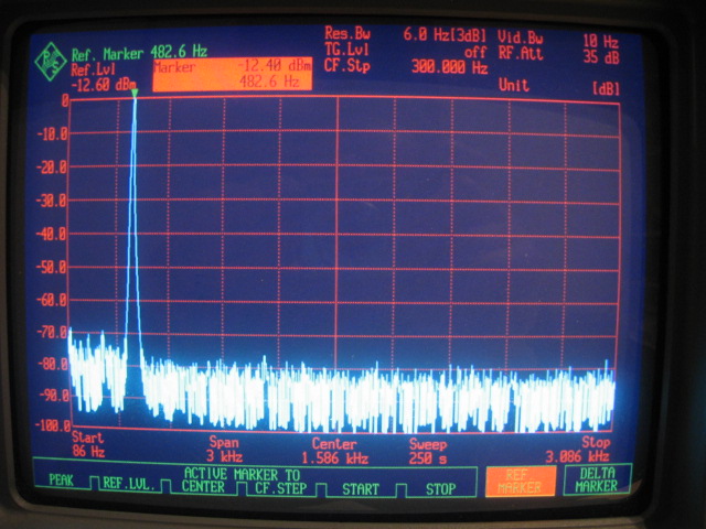
All harmonics of 482Hz are below the noise floor and only a non-harmonically related spur at 1211Hz can be seen peaking just above the noise floor. Higher order harmonics are not visible. Note the near absence of any power supply mains related hum and its harmonics.
The above measurements are done with the line-out output(s). The TS486 headset amplifier used is specified at 0.3% distortion, probably at maximum output level (100mW), but the datasheet is not very clear. Nevertheless little to no distortion is found. The TDA7391 amplifiers used for the speakers are specified at 0.03% distortion for power levels < 15W. No attempt has been done to actually verify the distortion introduced by the TDA7391 PA's. The difficulty is the connection with the spectrum analyzer of the floating output port of these bridge topology amplifiers! A low frequency transformer could be used or an instrumentation amplifier to solve this. However given the specified linearity of these amplifiers and the typical output power that will be needed this path has not been further explored.
The final source of IMD and other distortion will be the speaker system or headset. To investigate this is a project on its own and rather out of scope for a radio amateur! It is probably a good idea to complement the signal path with a pretty good set of external speakers boxes and a quality headset!
Assembly
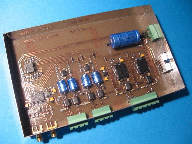
The first prototype of the Audio Board, fully assembled in its tin metal box, is depicted in the photo below.
The module is euro-card sized and follows the general layout rules used consistently in this project:
-
Power and I2C control connector are located at standard positions at the right edge of the board.
-
SMA connectors and others are located at the bottom edge of the board and provide the signal interface to the board.
The board contains the following sub-circuits, which can be recognized from the picture:
-
TDA7309 analog audio processor.
-
TS486 line-out amplifier.
-
TS486 headset amplifier.
-
2x TDA7391 power amplifiers.
-
I2C hardware to control the board through I2C with a microcontroller.
-
On-board voltage regulators and extra power supply filtering.
Adjustment
No on-board "analog" adjustments are needed to commission the Audio Board. It is of course possible to tweak the voltage gain of the line-out amplifiers and the headset amplifiers with resistors R23, R22, R26, and R27 depending on your preference.
Solder jumpers SJ1, SJ2, SJ3 and SJ4 determine the I2C addresses of IC1 and IC8. They should be configured such that there are no conflicts on the I2C bus with the addresses of other I2C chips.
Solder jumpers SJ5 and SJ6, which enable I2C-bus terminating resistors R10 and R11 should only be soldered in if the Audio Board is positioned at the end of the physical I2C-bus.
Documentation
The following link points to the Audio Board documentation file available for download for those who wish to reproduce the unit:
Audio Board documentation in PDF format
This PDF contains:
-
Schematics.
-
Bill of materials.
-
Component side, scale 1.6.
-
Back side, scale 1.6, showing the tracks to be wired by hand.
-
Top side, mirrored scale 1.0, for PCB production.
-
Bottom side, mirrored scale 1.0, for PCB production if needed.
Specification
The following table summarizes the key parameters of the Audio Board:
| Audio Board Specs |
| Dimensions |
160 x 100 x 30 |
mm |
| Weight |
290 |
gr. |
| Positive Supply Voltage |
+13.5 to +15 |
V |
| Positive Supply Current |
160 |
mA |
| Positive Supply Current all amplifiers disabled |
17 |
mA |
| Input Impedance |
50 |
kΩ |
| Volume Control Range |
95 |
dB |
| Volume Step Size |
1 |
dB |
| PA maximum output power in 3.2Ω |
2x32 |
W |
| PA distortion < 15W output power |
0.06 |
% |
| PA voltage gain |
30 |
dB |
| Headset maximum output power in 16Ω |
2x100 |
mW |
| Headset distortion |
0.3 |
% |
| Headset voltage gain |
12 |
dB |
| Line-out distortion |
< 0.3 |
% |
| Line-out voltage gain |
0 |
dB |
This concludes the description of the Audio Board.
Back to Receiver Overview
Back to the TOC
|