Measuring sideband noise using a crystal notch filter
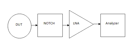
This method is described in detail by Wes Hayward, W7ZOI, in the July/August 2008 issue of QEX: "Oscillator Noise Evaluation with a Crystal Notch Filter". The idea behind it is to suppress the carrier with a very selective crystal notch filter, leaving only the noise sidebands to be inspected with a spectrum analyzer without overloading problems. My spectrum analyzer can be used to inspect the remaining noise sidebands up to -140dBm at best at its smallest RBW (3Hz), so at least an additional 40dB of amplification is needed to further amplify the noise sidebands behind the notch filter to be able to measure all the way down to the thermal noise floor at -174dBm. The block diagram of this measurement method is shown below:
Crystal Notch Filter
Following W7ZOI's recipe, a 5-pole crystal notch filter is designed using 5 of the remaining 14.31818MHz "AQ" crystals of the batch also used for the crystal filter with the reciprocal mixing method. The filter is based on the following elements:
-
The impedance is raised to 200Ω with transmission line transformers on small FT37-43 ferrite toroids to increase the notch depth.
-
5 crystals are used as shunt series resonators to produce the notch effect.
-
The 5 crystals are isolated from each other with 1/4λ lumped circuits, which are LC-π low pass networks. Xc and Xl are dimensioned to 200Ω at the crystal series resonance. All parallel shunt capacitors such as the crystals parallel capacitance and adjacent LC-π capacitors are collapsed in single capacitors optimizing and simplifying the design.
-
FT50-10 toroids are used together with polystyrene capacitors to obtain a high-Q circuit.
The performance of this filter is shown in the following network analyzer picture:
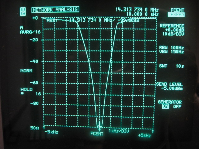
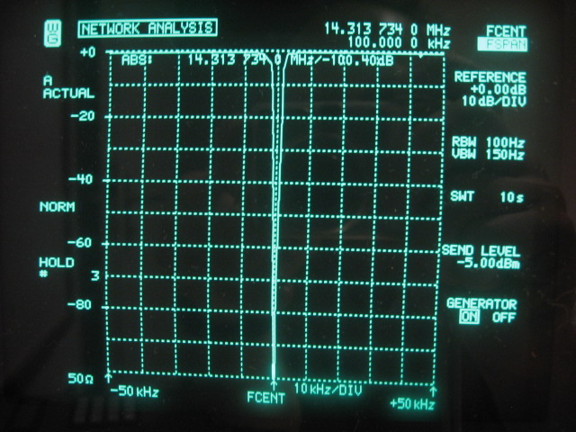
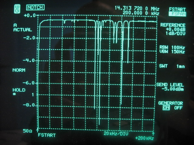
Ultimate stop-band at 14.313734MHz is measured at -111dB, which is remarkable because no extra metal shielding between the 5 sections has been used. The toroid inductors used in the 1/4λ lumped circuits are rotated 90° each to minimize leak through. The 14.31818MHz crystals have an average Q of 90000 and a motional resistance of 5.2Ω. The notch filter can be used to measure sideband noise at offsets greater than 2KHz. The following picture shows a much wider view of the same filter which demonstrates its selectivity:
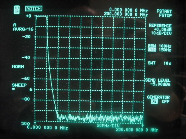
Nest is a picture showing a strong but secondary effect of the applied filter topology. It also happens to act as a very steep low-pass filter cutting-off at 18MHz. This is actually a good thing in this application, because it completely suppresses any harmonics of the carrier being measured. Those harmonics could otherwise possibly overload the spectrum analyzer, when amplified with the LNA by more than 40dB. The LPF effect is caused by the 4 lumped circuit 1/4λ sections that interconnect the 5 crystals.
The following picture shows a couple of spurious filter responses. One is almost exactly at 100Khz above the notch center frequency and is about 3 to 4 decibel deep. I originally used a 100KHz offset as one of the measurement points, which resulted in a 3dB error at that offset. Once this was discovered I started using a 90KHz offset instead of 100KHz to avoid the issue.
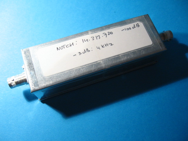
The following picture shows the crystal notch filter, build the "ugly" way inside a metal enclosure with BNC-connectors:
Low Noise Amplifier
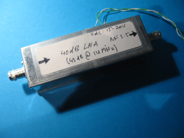
At least an additional 40dB of gain is needed between the crystal notch filter and the spectrum analyzer to overcome the noise figure of the analyzer. A simple LNA is build using 2 MAR6 MMIC's resulting in a very wideband and flat gain of 43dB with an estimated noise figure NF=3.5dB. The following picture shows the LNA, build SMD-style inside a metal enclosure with BNC-connectors:
Calibration
The crystal notch filter method is straight forward but a correction factor is needed to translate the values displayed on the spectrum analyzer to dBc/Hz values. The following points have to be taken into account:
-
The spectrum analyzers RBW (resolution bandwidth), must be corrected to 1Hz, when looking at noise. The correction is: -10 * log( RBW ). So -4.8dB for 3Hz, -10dB for 10Hz, -20dB for 100Hz RBW.
-
RBW is usually defined by the -3dB bandwidth of the Gaussian filter curve it represents. This is also the case with my SNA62. When the noise power is integrated over the characteristic shape of a Gaussian filter it will lead to slightly different results than with the ideal rectangular filter used normally in noise arithmetic. The correction is: RBWrect = 1.2 * RBWgauss. So the Gaussian shape is perceived by the noise as a slightly wider rectangular shape and the correction factor is -10 * log( 1.2 ) = -0.8dB
-
All spectrum analyzers are calibrated for displaying sinusoidal signals. Therefore a systematic error occurs when displaying noise power. The display of the spectrum analyzer reveals a level that is typically 2.5dB too small. So the correction to be made is +2.5dB.
-
The gain of the LNA must be taken into account. This correction is -43dB with the LNA used at 14MHz.
-
The insertion loss of the crystal notch filter must be taken into account. This is +3dB at 2KHz offset. It is negligible further out.
-
The level of the carrier that is investigated must be subtracted to arrive at dB's relative to the carrier: dBc/Hz values.
Apart from the offset dependent correction at 2Khz, the total correction factor becomes: Cf = -43 + 2.5 - 0.8 - 10 * log( RBW ) - Pc , so Cf = -41.3 - 10 * log( RBW ) - Pc , where Pc is the carrier level, which is close to 0dBm with the AD9910, and Cf is the correction factor in dB.
Armed with this calibration factor, have a look at the following analyzer shot which shows 5Khz around the DDS carrier after passing through the notch filter and the LNA:
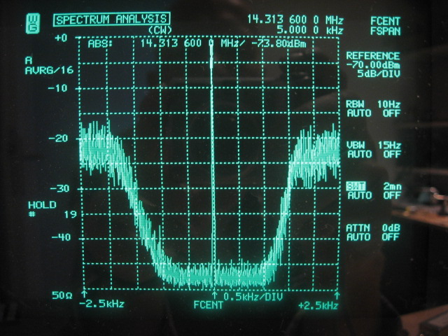
The strongest signal seen by the analyzer, the DDS carrier, is only -74dBm strong at the LNA output, which means that its level is actually at -117dBm at the output of the notch. With the carrier at -6dBm at the input of the notch with this particular measurement, this means that the notch suppresses the carrier with 111dB!
The plot has been made with 16 times averaging. The middle of the noise sideband corresponds to the average noise level in a 10Hz Gaussian RBW. At +2KHz from the carrier it is displayed as -95dBm on the analyzer. This translates to: -95 - 41.3 - 10 * log( 10 ) + 3 + 6 = -137.3dBc/Hz. 3 is added to correct for the insertion loss of the notch at +2KHz and -6 is subtracted to correct for the -6dBm carrier with this particular measurement.
We can also see the ultimate noise floor inside the notch stop-band at -117.5dBm on the analyzer. Using a correction factor of -41.3 - 10 * log( 10 ) = -51.3dB, the displayed noise floor translates into -168.8dBm before the LNA. The LNA has an estimated noise figure NF=3.5, so the real noise floor comes out at -172.3dBm, which is quite close to the thermal floor of -174dBm at room temperature. Most likely the NF of the MMIC's is slightly higher at 14MHz than the typical 3dB specified by Mini-Circuits at 0.5GHz.
The picture shows that the crystal notch filter method allows for sideband noise measurements all the way down to almost -169dBc/Hz, assuming a 0dBm carrier at the input of the notch. This is sufficient for evaluation of the AD9910 as a LO in a HF receiver. A better LNA could improve things a few dB, but it would have to be constructed from discrete components, because MMIC's with a NF=1dB don't seem to exist at HF frequencies.
Crystal notch filter pros and cons
The crystal notch filter method has the following characteristics:
-
A spectrum analyzer is needed. A crystal notch filter and LNA are also key components. Apart from that, the method is uncomplicated and straight forward.
-
The SSB noise of the signal being tested is measured directly.
-
SSB noise is measured consisting of PM-noise and AM-noise. The method does not have any preference to the kind of noise!
-
It is not possible to measure really close-in. The limitation is the bandwidth of the crystal notch filter. The practical limit with the notch I build is a 2KHz offset. Any closer-in requires a big correction with intimate knowledge of the transmission plot of the notch filter.
-
Because of the LPF effect, the possible maximum measurement offset is limited, when measuring above the notch frequency. The maximum offset possible with the notch I used is about 4MHz.
-
A crystal notch filter is needed. Therefore it can only be used at frequencies where a narrow crystal notch filter with good suppression can be practically designed. That range is probably limited by the use fundamental mode crystals at HF.
-
Spurious filter responses must be investigated and avoided as measurement offset frequencies.
-
Given a 0dBm signal and the NF of the LNA, down to -169dBc/Hz can be measured accurately using this setup.
Reciprocal Mixing
Crystal Notch Filter
Quadrature Mixing
Back to Sideband Noise Measurement
Back to the TOC
|