Quadrature Sampling Detector
Many options are open to implement a product detector at 9MHz. Examples are a (high level) ring mixer, a simplified H-Mode mixer with DC capable output or a Gilbert cell approach. For the Detector Board however the QSD circuit is chosen to act as product detector, because of its good linearity, I-Q outputs and low cost. Various varieties of the QSD circuit exist:
-
Single Balanced versus Double Balanced.
-
Using instrumentation amplifiers versus using OPAMP's.
-
Divide by 4 IQ-squarer versus Fundamental Hybrid IQ-squarer.
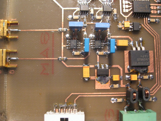
The following close-up picture shows the QSD section of the Detector Board including the BFO pre-amp and squarer. From this picture it can be deducted which particular QSD variety has been used!
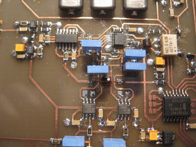
The QSD circuit found on the Detector Board is the double balanced version using instrumentation amplifiers and a divide by 4 IQ squarer. This choice seemed most appealing to me but surely any of the other options can be made to work fine as well.
IMD
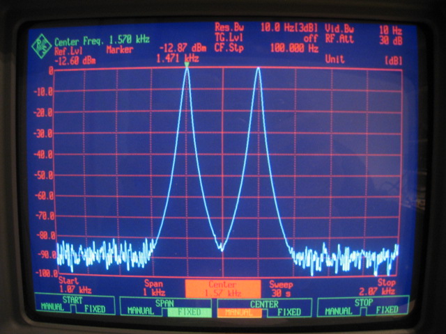
Well protected behind many poles of crystal filtering and at a nominal input level of -17dBm the linearity of the product detector need not be stellar. An IIP3 of only +10dBm is enough to provide -60dBc IMD levels at the -17dBm combined input level. The following photo depicts this situation with 200Hz spaced 2-tones. The IMD is well below the analyzer's 10Hz noise floor, probably at -100dBc. From a linearity point of view this is more than sufficient for this application, where the Variable Gain Board produces IMD3 at -60dBc.
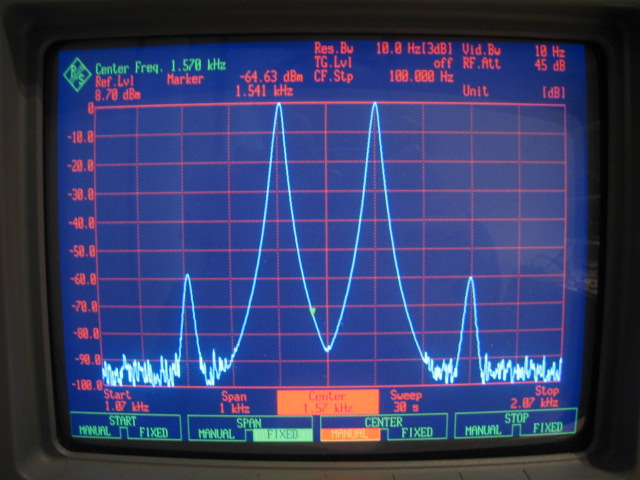
The following picture shows the IMD using 0dBm level input 2-tones. Now the IMD is exactly -60dBc, indicating an IIP3 of +30dBm.
It is maybe interesting to note that this +30dBm result was not obtained immediately in the first attempt with the QSD. Initially an IIP3 of only +10dBm was measured! This is much lower than can be expected from this circuit. It turned out that the quality of the four sampling capacitors is quite important for the end result. X7R MLCC's were used and this is a very poor component choice at this position. X7R dielectric is known for considerable voltage dependency, inevitably resulting in excess IMD. The fact that actually an IIP3 of +10dBm was reached with these capacitors says something about the quality of today's X7R MLCC's!
The situation is completely resolved using inexpensive through-hole MKT film capacitors. They have a polyester dielectric much more suitable for this application.
Sensitivity
Sensitivity represented by NF is extremely important if the QSD actually is the complete receiver's frontend without any gain preceding it. On the Detector Board however this property is not critical at all. The nominal input level at this point is -17dBm. Therefore no special ultra low noise instrumentation amplifiers are needed. The AD8221 is specified by Analog Devices at 8nV/√Hz @ 1KHz. Let's assume that this value is correct, then it is about 18dB noisier than the popular INA163 with its superb 1nV/√Hz. However given all the gain in front of the QSD this difference is completely irrelevant in this application. Therefore AD8221 is chosen as it is by any means a very precise, low distortion and low cost instrumentation amplifier. Although 1206 resistor pads are available for R1 and R2 on the PCB layout to set the gain of IC1 and IC2, they should not be mounted. This results in unity gain for both instrumentation amplifiers.
Although the instrumentation amplifiers are set to unity gain, the voltage gain of the QSD is still almost 4 times or 11dB. This is caused by the impedance transformation (x2) and the double balanced wiring (x2) of the detector. At -17dBm nominal input level the Detector Board has sufficient output signal to drive the Audio Board.
Bandwidth
The QSD is not a conventional mixer. It is really a sampling detector with a well defined detection bandwidth. Much has been written about this subject given its popularity in the SDR community, so it should be sufficient to note here that the detection bandwidth of the double balanced QSD depends on source impedance and capacitor value in the following way:
BWdet = ( 2⋅π⋅Rs⋅Cs ) -1
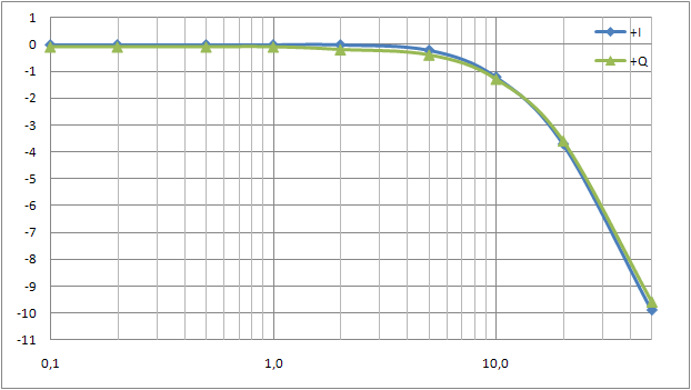
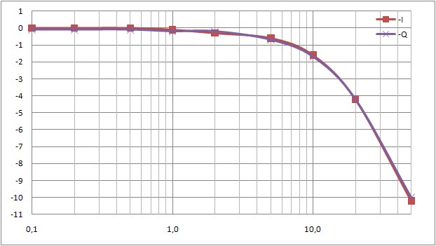
Given the components (Cs=22nF, input transformer and 100Ω resistors) this should result in a -3dB bandwidth of approximately 18KHz. The following graph shows the measured detector response. The red curve represents the I output relative in dB to its maximum as a result of a positive frequency offset in KHz (Fin > Fbfo). It completely overlaps the blue curve which is the response to a negative frequency offset (Fin < Fbfo).
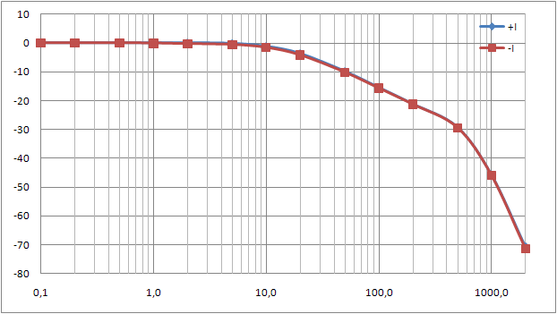
The first -3dB cut-off point corresponds well with the theoretical 18KHz and almost -6dB/octave is obtained. At 600KHz there is a second -6dB/octave action kicking in. This is caused by the bandwidth of the instrumentation amplifier. The bandwidth of the AD8221 in unity gain configuration happens to be 600KHz.
The QSD bandwidth of 18KHz is much more than needed for our widest modulation method: SSB. The IQ outputs are followed by a pair of 2-pole unity gain active filters. The Butterworth response -3dB cut-off point is set at 3.3KHz. At 2.4KHz the gain is -1dB, which ensures a flat response of the QSD board for SSB signals. LME49710 low noise low distortion audio OPAMP's are used which add negligible noise and distortion. Components in both channels are selected for equality to not disrupt the balance of the IQ outputs.
The picture below zooms in on the section of the Detector Board that holds the low pass filters and the positive and negative supply LDO regulators. Note that also MKT capacitors are used in the low pass filters although test with NP0/C0G MLCC's showed no additional IMD.
IQ Amplitude Balance
When the IQ outputs are used in an image rejection application, be it in hardware or in software, then amplitude and phase balance are very important. Although slight errors can be compensated in software it is interesting to see how much balance can be easily obtained with the QSD circuit. Assuming near identical instrumentation amplifiers and near identical Ron of the FSA331 multiplexer switches, the 4 sampling capacitors will largely define the amplitude error. From a random batch of 20 MKT 22nF polyester film capacitors it was possible to select 4 capacitors with nearly identical values. Three were within 0.1% and one was within 0.3% of 23.5nF. The following graph shows the frequency response in dB of I and Q for Fin > Fbfo (KHz). Both curves nearly overlap and are within 0.1dB identical.
Given the properties of the circuit exactly the same result is also achieved Fin < Fbfo. Both curves again are within 0.1dB identical as shown in the following picture:
The above results show that relative accuracy of the capacitors is a key factor in getting amplitude balance with the QSD. There is no need for absolute accuracy of the sampling capacitors, so selecting 4 from a larger badge of cheap polyester stuff will do well. Also temperature sensitivity is not very important as all 4 capacitors will have the same temperature.
IQ Phase Balance
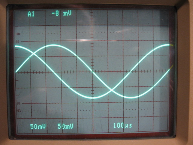
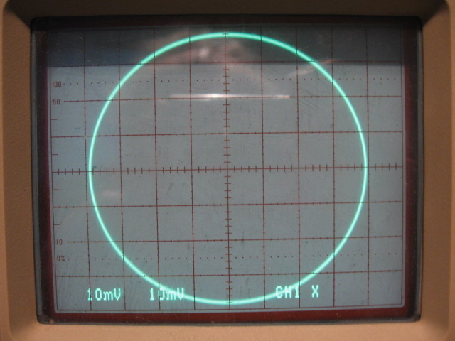
How about phase balance? Given that all components are balanced and a synchronous divide by 4 Johnson counter is used to drive the multiplexer, there should not be much phase unbalance! The following picture shows I and Q for a 1KHz output signal. Amplitude looks identical and the zero crossing of the cosine is exactly at the right spot at 250μs.
A cosine and sine wave together should result in a perfect circle when driving the X and Y channels of the oscilloscope. The following picture shows the result, a near perfect circle:
I have not yet measured the image rejection possible without any software calibration with this QSD using an SDR software package. It should be good.
BFO pre-amplifier
A simple grounded gate JFET amplifier is used to amplify the 36MHz BFO signal to clock the Johnson counter. About 6dB voltage gain is reached with this configuration. This enables reliable clocking of the QSD for BFO input levels in between -15dBm and +12dBm. With more than +12dBm input level the gain of the preamp should be reduced otherwise the output voltage exceeds the Vcc of the 74AC74. A BFO level between -6dBm and 0dBm is about perfect. This means that the Detector Board can be clocked directly with the filtered DAC output of an AD9951 or AD9910/12 DDS chip.
Conclusion
The QSD circuit can be made to perform extremely well with readily available off the shelf components. Because of its good linearity, its in-channel IMD contribution is negligible at this point in the signal path. Its IQ outputs allow easy interfacing with popular PC based DSP software or can be simply used for binaural listening.
The schematics and part list of the Detector Board prescribe an FSAV331 video switch from Fairchild. This part happened to be available. Probably most members from the '3253' family of 2x 1:4 Mux/DeMux bus switch such as FST3253, PI5C3253 and other equivalents will do fine as well. The PCB layout however only accepts an equivalent part in a QSOP-16 package!
Please follow the links below to read more about the Detector Board.
Noise Filters
Quadrature Sampling Detector
Back to Detector Board
Back to the TOC
|