Introduction
The subsystems presented so far have in common that they all use on-board LDO voltage regulators to provide the supply voltages needed to power the circuits they contain. Most boards have an internal +12V rail. Some also have a -12V rail. Sometimes lower voltages are derived from these rails with subsequent regulators to produce +9V, +7V, +5V and -5V. The only exception is the Audio Board where the stereo power amplifiers are powered directly from the +14V input supply rail.
The onboard voltage regulators are all Low-Drop-Out. They can operate with a relative small drop in voltage between input and output. Usually a difference of only 1V between input and output is more than sufficient headroom for these regulators to perform well. It is important to keep the main supply voltages close to +12V and -12V with just enough margin for the onboard LDO's to operate properly in order to keep the dissipation as low as possible. This is especially true for the Variable Gain Board, which is the most power hungry board in the signal path! In practice somewhere between 1V and 2V of margin gives good results:
-
Low onboard dissipation.
-
Good secondary onboard voltage regulation.
This calls for the following supply voltages:
-
+14V. Used to power +12V onboard LDO regulators.
-
-14V. Used to power -12V onboard LDO regulators.
-
+18V. Used to power the +15V onboard regulator for the Wenzel 100MHz OCXO reference oscillator.
-
+5V. Used to directly power the digital circuits like DDS's, Controller(s) and Graphics Display.
Differences in load and also big variations in AC mains voltage are possible. It seems not very feasible to reliably power the subsystems with an unregulated power supply, always between 1V to 2V above the internal voltage rails. The 100Hz ripple alone could easily account for 0.5V already! In case of the +12V internal rail an external voltage is needed of +14V maximum that never dips below +13V regardless of external and internal conditions. What is needed is an efficient pre-regulator that can supply +14V within the margins needed. This is where the Switcher Board fits in. The main objectives of the Switcher Board are to provide:
-
4 supply voltages including a negative voltage from a single unregulated supply.
-
Efficient pre-regulation of the 4 main supply voltages.
-
Over current protection of the 4 main supply voltages
-
Crowbar like over voltage protection of the 4 main supply voltages
-
Under voltage protection.
-
Simple pushbutton like On/Off control.
-
Handshaking with the main MCU for housekeeping in software just before Power Off.
Block Diagram
The main purpose of the Switcher Board is to efficiently supply the 4 main supply voltages with good regulation and minimal ripple from a single unregulated supply voltage. The block diagram below shows the approach in more detail:
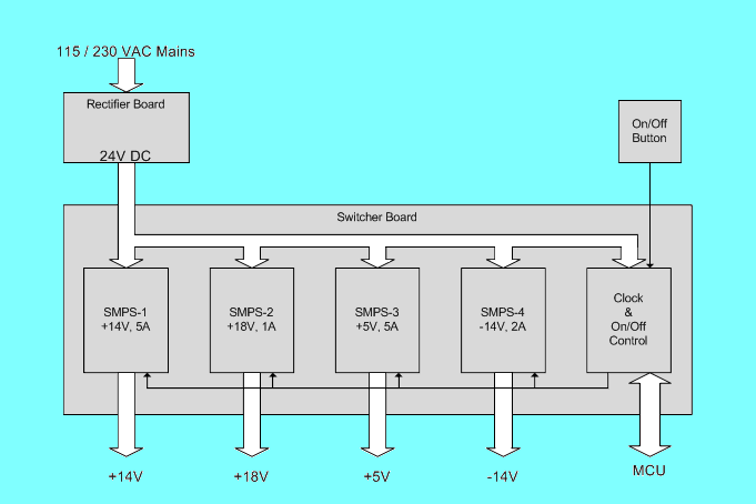
The mains AC voltage is transformed and rectified the conventional way with a heavy 50Hz toroidal transformer followed by a 2-phase rectifier into a raw 24VDC single supply rail. Only one transformer with one rectifier and large C reservoir is needed. The nominal 24VDC is chosen such that two standard 12V batteries in series could also power the Switcher Board.
The Switcher Board uses 4 independent switching regulators to deliver the required output voltages. The efficiency of this solution is very good. The biggest loss in power is probably due to the rectifier and the transformer on the Rectifier Board. Three of the four switchers are BUCK step-down switchers. They convert +24V into +14V, +18V and +5V. The remaining switcher is a BUCK-BOOST inverter to convert +24V into -14V.
From the block-diagram it can be seen that the +24V raw unregulated supply is always enabled. SMPS-2, the +18V switcher is also always enabled. It powers the ovenized 100MHz reference oscillator which is best left running all the time to obtain high stability and long life. Of course there is the possibility of a power switch at the back side of the cabinet to power off completely. The remaining switchers, SMPS-1, SMPS-3, SMPS-4, are enabled / disabled by means of a push-button control. This functionality is captured by the Clock & On/Off Control block.
Rectifier Board
The following picture shows the Rectifier Board with the mains transformer and filtering that provides the +24V unregulated raw DC voltage to the Switcher Board.
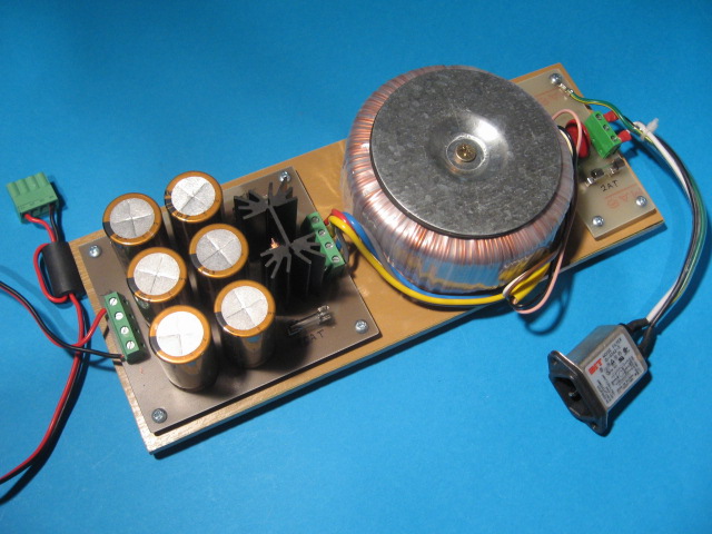
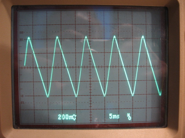
The mains transformer is a 225VA 2x20V (5.62A) toroidal transformer. It provides more than sufficient power to also power the transmitter in the future even with a medium power PA. The 2-phase rectifier consists of a Schottky diode pair with minimal voltage drop, but still a noticeable heat-sink is required to prevent a meltdown of the rectifier during extended time of full power (180W) with a 100% duty cycle. The capacitor reservoir consists of 6x10000μF. Each capacitor can handle 4A of ripple current. In simulation the RMS current at full load in the combined 60000μF capacitor is close to 10A. That is 1.67A per capacitor. The following picture shows the ripple voltage of this configuration at full load:
Without the future transmitter and its associated power amplifier the presented Rectifier Board solution will be significantly "over-engineered". This results in more weight and more space but also in very little heat. The additional cost of the heavy transformer is actually not too significant. 120VA: 45.87€, 91mmx49mm, 1.4kg. 225VA: 58.01€, 110mmx52mm, 2.3kg. Sometimes this part is under-engineered resulting in a frighteningly hot transformer under long lasting heavy load. Of course the Rectifier Board can be scaled down to personal taste! Size is probably a non-issue if the Rectifier Board is kept outside the rig's cabinet. This also simplifies powering the rig with 2 batteries as an alternative to AC mains.
Apart from the heavy duty PSU components there is also additional filtering visible on the first picture. The 24VDC is RF-choked with a big 2-turn common mode ferrite tube preventing switching energy to leave the Switcher Board. The ferrite tube has been scavenged from a broken computer CRT display, which is often a good source of EMI ferrites. On the primary side a built-in mains filter is used and additional surge protection is added with a big red MOV and a 1.5KW bipolar TVS diode. Primary and secondary sides are both fused and the secondary side of course in both phases before the big reservoir.
Switcher Board
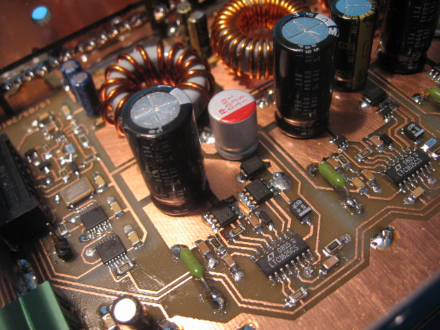
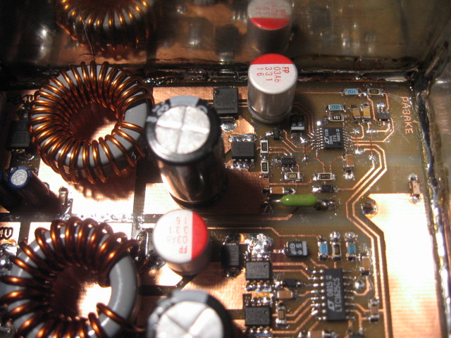
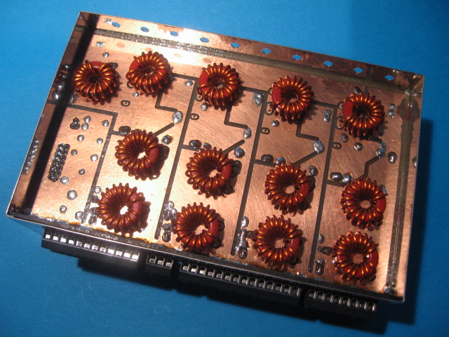
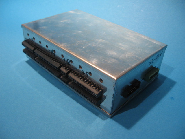
The following picture shows the completed Switcher Board in its tinned metal box.
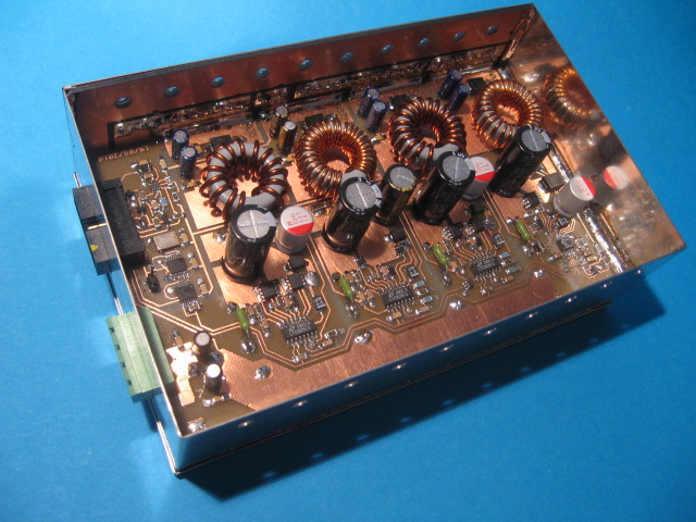
The PCB is subdivided in 5 slices with the following functionality:
-
Clock & On/Off Control.
-
+5V buck step-down converter.
-
+18V buck step-down converter.
-
+14V buck step-down converter.
-
-14V buck/boost inverter.
Clock & On/Off Control
The On/Off pushbutton function is implemented with IC8, LTC2950-1. This IC performs the following 3 On/Off related functions:
-
Reliable On/Off switching with a simple pushbutton of the +14V, -14V and +5V switchers.
-
Under voltage protection. Below 21.0VDC input voltage the 3 switchers are disabled.
-
Optional handshaking with the MCU that controls the rig to provide the possibility to do housekeeping in software just before power Off. The handshaking can be disabled by soldering solder jumper SJ1.
Apart from the On/Off function this block also generates a common clock signal used to drive all 4 switchers. The clock is derived from a standard personal computer VGA pixel rate and low cost 18.432MHz crystal oscillator and is divided down by 94 or 96 to obtain the final switching frequency of 196Khz or 192Khz. The reason to synchronize all 4 switchers to the same stable clock is to minimize any spurs in the receiver caused by the switching pre-regulators. By using the same crystal derived clock signal for all switchers instead of their internal RC oscillators, there will be 1 set of spurs instead of 4 sets. Furthermore this single set of spurs is crystal driven, so it is well defined and will not drift around much at all.
The black 14 pin flat-cable connector exposes the Clock & On/Off Control external interface:
-
SYNC. Output: 192KHz or 196KHz TTL clock signal intended to drive additional switchers if needed.
-
47/48. Input: Used to select the switcher clock frequency. Logic '1': 192KHz, Logic '0': 196KHz.
-
ENABLE. Output: Logic '1' if switchers are "On", Logic '0' if "Off"
-
INT. Output: Positive edge to be used to trigger interrupt with MCU when powering down with the pushbutton.
-
KILL. Input: To be pulled high by the MCU within 1024ms after INT goes high to confirm the shutdown.
-
PB. Input: Should be connected to the On/Off pushbutton.
For further details please look up the Switcher Board schematic and the datasheet of the LTC2950-1.
BUCK step-down converters, +5V, +14V, +18V
The next picture shows a close-up from left to right of the Clock & On/Off Control block, the +5V switcher and the +18V switcher:
The +5V, +18V and +14V switcher circuits are very similar to each other and mainly differ in the component values of L and C and the MOSFET switches. The SMPS controller IC used is the LTC1625CS by Linear Technology. The LTC1625 implements a synchronous step-down switching regulator. The 3 switchers are almost 100% application-note circuits. The datasheet is very helpful in providing the information to properly dimension the L, C and MOSFET's. The following table gives more details of the dimensioning of these switchers:
| LTC1625 BUCK step-down switching regulators |
|
+5V SMPS |
+14V SMPS |
+18V SMPS |
Unit |
| Fswitch |
192 or 196 |
192 or 196 |
192 or 196 |
KHz |
| Vin |
27 |
27 |
27 |
V |
| Vout-design |
5.00 |
14.00 |
18.00 |
V |
| Vout-practical |
5.00 |
13.92 |
17.85 |
V |
| Iout-max-design |
5 |
5 |
1 |
A |
| Iout-max-practical |
4 |
4 |
1 |
A |
| Iout-short-cut |
1.90 |
1.73 |
0.37 |
A |
| ΔIl-max |
30 |
30 |
40 |
% |
| ΔIl-max |
1.5 |
1.5 |
0.4 |
A |
| Il-peak |
5.75 |
5.75 |
1.20 |
A |
| Ilimit |
5.50 |
5.50 |
1.05 |
A |
| Iin |
0.96 |
2.63 |
0.68 |
A |
| Irms-Cin |
1.94 |
2.50 |
0.47 |
A |
| ΔVout-max |
10.5 |
10.5 |
7.6 |
mV |
| Cin |
1000 |
1000 |
1000 |
μF |
| Cin-ESR |
15 |
15 |
15 |
mΩ |
| Cout |
330 |
330 |
680 |
μF |
| Cout-ESR |
7 |
7 |
19 |
mΩ |
| Magnetic-Core |
55310A2 |
55310A2 |
55310A2 |
|
| L-design |
14.15 |
23.41 |
78.13 |
μH |
| L-full-load |
15.06 |
24.99 |
82.80 |
μH |
| L-no-load |
17.64 |
32.49 |
86.49 |
μH |
| Turns |
14 |
19 |
31 |
# |
| Wire-thickness |
1.6 |
1.6 |
1.0 |
mm |
| Core-temperature-rise |
7.4 |
9.7 |
3.0 |
°C |
| Crss |
100 |
100 |
30 |
pF |
| Rds-on-design |
18.46 |
18.46 |
92.31 |
mΩ |
| Rds-on-practical |
20 |
20 |
100 |
mΩ |
| Power-out-design |
25 |
70 |
18 |
W |
| Ploss-top-MOSFET |
242 |
442 |
87 |
mW |
| Ploss-bottom-MOSFET |
402 |
212 |
25 |
mW |
| Ploss-core |
135 |
215 |
53 |
mW |
| Ploss-copper |
105 |
143 |
22 |
mW |
| Ploss-cin |
60.4 |
99.9 |
3.6 |
mW |
| Ploss-cout |
3.9 |
3.9 |
0.8 |
mW |
| Ploss-total |
949 |
1115 |
192 |
mW |
| Efficiency |
96.3 |
98.4 |
98.9 |
% |
For those not familiar with switched-mode power supplies, it is a good idea to read through the LTC1625 datasheet and most of the rows in the table above will make more sense. The dimensioning and component properties of L, Cout and the MOSFET's are the most important part in the design of the circuit. The Cin and Cout switching reservoir capacitors need to be of very good quality. Especially low ESR and high maximum allowable ripple current are important properties. If the exact same parts cannot be obtained, make sure the replacements are similar with respect to these properties!
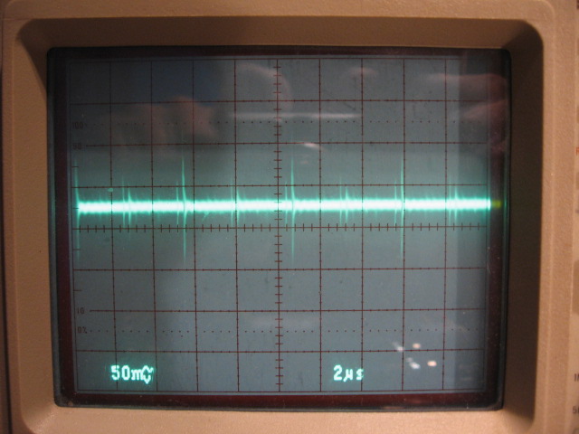
The ESR of the Cout reservoir capacitor is especially important and the ripple output voltage of the switcher is almost directly proportional with its ESR value. Nichicon Aluminum Organic Polymer capacitors with extremely low ESR (7mΩ) have been used for the +5V and +14V switchers. This type of capacitor is not available for voltages above 16V, so for the 18V switcher a low ESR aluminum electrolyte has been used. The following picture shows the ripple voltage called ΔVout-max in the table for the +14V switcher at full load (4A):
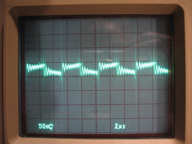
The ripple voltage is about 30mVtt which is more than the predicted value of 10.5mVtt for this switcher. The LC filter following the BUCK switcher does significantly reduce the ripple experienced outside the Switcher Board. This is discussed in more detail in the "Switcher Spurs" section on this page.
The story on the selection of the switching inductor core could be a chapter on its own. Specialized magnetic materials have been developed to give the best properties for switched mode power supply applications for different frequency ranges. The iron powder materials 2, 6, 10 used for HF resonant circuit applications such as our BPF-box are not really suitable for this application. Micro Metals does provide iron powder cores suitable for 190KHz switchers with the 52 material toroids. However core losses are still quite noticeable with this material so other alternatives have been looked at in order to keep the cooling requirements of the switcher board as low as practically possible.
Magnetics Inc. manufactures toroids made of what they call MPP material (Magnetics Molypermalloy Powder) which are quite expensive ($3.85 for a T94 sized 55310A2 core versus only $0.80 for a T94-52), but gives excellent low core loss results and have been tested with the Switcher Board. However acceptable results should be possible too with Micro Metals T94-52 cores. With T94-52's, use 17 turns to obtain 14μH at the required DC bias for the +5V switcher, use 23 turns to obtain 23.4μH for the +14V switcher and use 38 turns to obtain 78μH for the +18V switcher. MPP material gives much lower magnetic core losses for the same core size and also less reduction in permeability at the same DC-bias resulting in less turns and therefore also less copper losses. In practice when testing at full load for half an hour the MPP cores barely get warm, which was exactly the intended result. T94-52 core simulations give almost 6 times higher core losses with the +5V switcher and 12 times higher losses with the +14V switcher, which means that they will get quite warm at full load. This has not been tested on the Switcher Board so far.
The LTC1625 controller is designed for high efficiency switchers and therefore a discrete lossy current sensing resistor has been eliminated. The Rds-on of the top MOSFET switch is used as the current sensing resistor instead. This trick improves efficiency but makes the choice of the MOSFET more critical. The table shows that 18.5mΩ Rds-on is the ideal value for the (top) MOSFET in case of the +5V and +14V switcher. Fairchild FDS5680 with 20mΩ comes close and is selected. Other logic level MOSFETS with similar Vds, Ids and Crss, packaging and pinning will do too. The +18V switcher requires close to 100mΩ Rds-on and the Siliconix SI3458DV is found to be suitable. Note that the common 30V logic level MOSFETS are to be avoided as their maximum Vds is too close to the unloaded +30V output voltage of the Rectifier Board. They will work but probably not with high reliability. A failing MOSFET is a disaster as the full 24V unregulated voltage could appear at the switchers output! This is discussed in more detailed in the "Over Voltage Protection" section on this page.
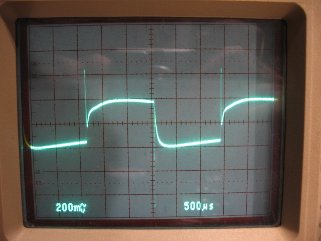
The following picture shows the transient behavior of the +14V switcher when the load is switched between completely off and full load (4A). There is a 140mV drop in output voltage during the full load condition, but the response of the switcher is very fast, about 100μs. The voltage drop is mainly caused by the copper losses in the wiring and LC filters outside the feedback loop.
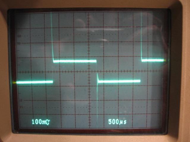
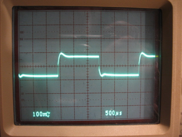
Note the strong spikes at the on/off boundaries! These spikes are largely caused by the additional LC output filtering that follows the BUCK switcher. With a low ESR 1000μF electrolytic capacitor directly over the switched load the spikes are removed and the result looks like this:
BUCK/BOOST inverter, -14V
While the previously described step-down switchers are nearly out of the box application-note circuits using the LTC1625, the inverter required to BUCK/BOOST the raw unregulated +24V into -14V is a slightly different story. The reason for this is that there are not that many integrated solutions available that can actually do this! None of the BUCK/BOOST inverter IC's found so far could handle the 30V raw unregulated input voltage. Some SEPIC topology controllers can do it, but not synchronisable at 192KHz, which is required. One of the related difficulties with the SEPIC inverters is that they require a bipolar capacitor, which is usually implemented with special but expensive MLCC's only affordable at much higher frequencies than our 192KHz.
A solution is found by using a standard asynchronous controller IC, usually used for BUCK step-down switchers capable of handling the 30V raw input voltage. An asynchronous controller can be easily externally adapted to support a BUCK/BOOST inverting topology. The LT3844 by Linear Technology is suitable for this. It is asynchronous, just 1 MOSFET output driver, which is normally used to switch a high-side N-channel MOSFET in a classic BUCK configuration, where the second switch is implemented the asynchronous way with a Schottky diode. However there is a problem that the integrated N-Channel floating driver is not useable with this inverting topology. The reason is that the controller's SW pin, used to help float the driver with respect to the MOSFET's source with an additional boost capacitor, is not designed to handle the negative voltage when the switch is open! If the output driver can be made to drive a high-side P-channel MOSFET, whose gate is driven relative from Vin, then the LT3844 can be fooled to act as a BUCK/BOOST inverting switcher, something it was not designed for!
For this to work the integrated N-channel driver is disabled partially so the driver output is now just a logic output above ground. An external discrete high-side P-Channel driver is added. This is done with the Q8, 2N2007, inverting stage and the classic bipolar totem-pole output driver with the NPN/PNP pair Q11. This driver is more than fast enough to switch a big P-Channel power MOSFET at a few hundred KHz.
One more issue must be solved as the LT3844 feedback pin expects a positive voltage instead of the negative voltage available now! This is handled by IC5, LT1783, a low power rail-to-rail OPAMP, which inverts the negative -14V output into a positive voltage accepted by the feedback pin of the LT3844. This closes the loop. The following picture shows the -14V switcher (top) and +14V switcher partially (bottom):
Fiddling with an external discrete MOSFET driver, outside the comfort-zone of a tested integrated solution backed-up by a fully tested application-note circuit, comes with some extra risks and care for details is needed otherwise smoke is inevitable! This is certainly valid with this circuit too. There is a chance of nearly instantly frying the P-Channel MOSFET switch, if the driver circuit is not able to completely drive the MOSFET into saturation. This situation is possible when Vin is low enough. And this occurs briefly each time we turn on the supply! For Vin less than 10V, the driver can only supply 5V Vgs at best. This is sufficient for logic level MOSFET's, but for Vin < 10V however the situation is becoming increasingly problematic.
Unintentional but easy reproduction of the problem showed when applying the input voltage in the first tests by manually ramping up Vin slowly from 0 to 30V. This "careful" approach actually caused things to blow up quite easily! The solution is found in preventing the LT3844 driving the switch by enabling the chip only if sufficient input voltage is present. Although under voltage protection functionality is present in the LT3844, it is implemented in a different way on the Switcher Board with the already available enable function of the LTC2950-1 pushbutton controller. The LTC2950-1 solution is preferred because it enables/disables all three switchers simultaneously. R33 and R24 at the "KILL" pin are dimensioned such that under voltage protection kicks in below 21.0V with 0.7V built-in hysteresis, so 21.7V is needed to be able to enable the switchers. This fairly high lowest acceptable input voltage is chosen in order to be able to guarantee the +18V switcher output that drives the rigs 100MHz reference oscillator.
The following table gives more details of the dimensioning of the -14V inverting switcher:
| LT3844 BUCK/BOOST inverting switching regulator |
|
-14V SMPS |
Unit |
| Fswitch |
192 or 196 |
KHz |
| Vin |
27 |
V |
| Vout-design |
-14.00 |
V |
| Vout-practical |
-13.91 |
V |
| Iout-max-design |
2 |
A |
| Iout-max-practical |
2 |
A |
| Duty-cycle-max |
38.1 |
% |
| Duty-cycle-min |
35.3 |
% |
| ΔIl-max |
30 |
% |
| ΔIl-max |
0.93 |
A |
| Il-avg |
3.23 |
A |
| Il-peak-peak |
0.88 |
A |
| Il-peak |
3.67 |
A |
| Iin |
1.13 |
A |
| Irms-Cin |
1.88 |
A |
| Irms-Cout |
1.57 |
A |
| Vdiode |
0.6 |
V |
| Vsense-max |
0.13 |
V |
| Vswitch |
0.1 |
V |
| ΔVout-max |
6.17 |
mV |
| Cin |
1000 |
μF |
| Cin-ESR |
15 |
mΩ |
| Cout |
330 |
μF |
| Cout-ESR |
7 |
mΩ |
| Magnetic-Core |
55310A2 |
|
| L-design |
53.52 |
μH |
| L-full-load |
55.55 |
μH |
| L-no-load |
70.56 |
μH |
| Turns |
28 |
# |
| Wire-thickness |
1.0 |
mm |
| Core-temperature-rise |
11.7 |
°C |
| Crss |
50 |
pF |
| Rds-on-practical |
100 |
mΩ |
| Rsense-design |
21.68 |
mΩ |
| Rsense-practical |
22 |
mΩ |
| Power-out-design |
28 |
W |
| Ploss-MOSFET |
554 |
mW |
| Ploss-diode |
1253 |
mW |
| Ploss-core |
187 |
mW |
| Ploss-copper |
194 |
mW |
| Ploss-cin |
53.1 |
mW |
| Ploss-cout |
17.2 |
mW |
| Ploss-sense |
226 |
mW |
| Ploss-total |
2.49 |
W |
| Efficiency |
91.9 |
% |
The full power efficiency of just 92%, although sufficient, is much lower with the inverting BUCK/BOOST topology than what is achieved with the previous 3 switchers. There are a couple of causes:
-
The higher switching current is caused by the inverting topology and causes more losses in MOSFET, resistor, inductor and capacitors.
-
The Schottky diode needed for asynchronous operation has a higher voltage drop and is less efficient than a synchronously switched MOSFET switch.
-
The P-Channel power MOSFET has much higher Rds-on than a similar N-Channel power MOSFET.
-
The additionally required Rsense resistor adds to the losses as well.
Instead of the low loss MPP 55310A3 core also an iron powder T94-52 can be used at the cost of increased losses. The number of turns in that case should be 34 to obtain 53μH at the given DC-bias.
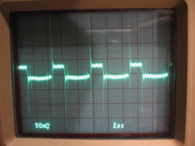
The following picture shows the ripple voltage on the Cout reservoir capacitor at full load. The 40mVtt ripple is more than the theoretically anticipated 6.2mV.
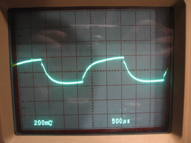
The next picture shows the transient response to switching the load between full load and no load. The inverting topology has much slower transient response than the BUCK step-down convertors described earlier. This is not a major issue as the -14V rail is mainly used to power the negative supply of OPAMPS and AD600's which are constant current sinks. Note once again the spikes mainly caused by the additional filters outside the control loop.
Applying an additional low ESR 1000μF capacitor directly over the switched load solves the spikes but shows the slower transient response more clearly:
Over Voltage Protection
With certain types of voltage regulators there is always the possibility of catastrophic failure causing the unregulated supply voltage to damage all attached circuitry. This has always been a risk with traditional series regulators, and is certainly not less risky with BUCK step-down switchers. If the high-side N-MOSFET becomes short circuited it means disaster! In the case of a BUCK step-down converter the risks are to be taken quite serious as the unregulated input voltage is often much higher than the intended regulated output voltage. There will be no survivors if 27V reaches 5V digital circuits.
LTC1625 does have an output overvoltage comparator which opens the top switch and closes the bottom switch if the output voltage is found to be out of control. But what good is that in case of the most likely scenario for over-voltage caused by a short circuit in the top MOSFET? Certainly the bottom MOSFET will also meltdown, causing a complete short circuit to ground for Vin. This will blow the fuses on the Rectifier Board, but they have to be slow to survive the turn-on transient of charging the empty 60000μF reservoir. Therefore a large surge may still materialize at the output of the switcher.
Protection for such a scenario is often provided by a crowbar circuit where the over voltage triggers a big thyristor that short circuits the unregulated supply blowing its fuses. This sounds easier than it actually is. The thyristor should not trigger on a very short temporary pulse, so a certain time delay has to be built in. Spice simulations with thyristor crowbars showed that still a significant surge can be expected at the output. Also the component count for 4 crowbar circuits on the Switcher Board is problematic.
Therefore a different approach is explored and implemented for all 4 switchers. Each output is simply protected by a matching 1.5KW TVS diode. (Transient Voltage Suppressor). TVS diodes can be seen as specialized very fast zener diodes. The SMCJ14A for instance has a breakdown voltage of 15.6V and is used to protect the 14V supplies. It can handle a very large peak current when it breaks down. In addition to that each switcher is also individually protected by a very fast 5A fuse to limit the current that it can sink from the 24V unregulated supply on failure. The fuse used is a 5A PICO-II fuse, which is a soldered through hole part on the PCB. On the pictures it can be identified as the green resistor like component. These fuses will blow in < 4ms at 10 times its rated current. This will be the case when the TVS diode is given a voltage in excess of its breakdown voltage and / or when the MOSFET's meltdown. Spice simulations show that the TVS diode protects external circuits better than the SCR crowbar because of its very fast reaction time. This is especially the case with short pulses where an SCR crowbar offers no protection for at all.
However, also with a TVS diode there will still be a short surge leaving the Switcher Board on catastrophic failure. For the +14V, -14V, +18V supplies this will not be a major problem as most of the circuits powered by these supplies have onboard secondary LDO regulators that should be able to handle this gracefully. The +5V supply however powers digital circuits directly and a risk of damage is not completely preventable. The SM5908 TVS diode used for that rail has a breakdown voltage of 6V. Hopefully it will never be needed to have the over voltage protection kick in dramatically, but make sure to order a couple of extra PICO fuses, just in case. All 4 switchers have been significantly over-engineered with the aim of high reliability. In practice with only the receiver running, the temperature of the Switcher Board box barely rises.
Not the same but related to over voltage protection is also short circuit protection. The three BUCK step-down switchers have a built-in current fold-back protection in case of too much output current. This provides a lot of safety for the various modules they power. A short circuit in one of the boxes does not pull the full peak current from the Rectifier Board, which would be sufficient for small spot welding jobs! Instead a reduced current, about 50% of its maximum at almost 0V, is delivered, which is not enough power to damage PCB's or cause smoke. The -14V switcher does not have current fold back and delivers about 4A under a short circuit condition, which it can sustain without overload.
Switcher Spurs
A very important subject when using switching power supplies are the spurs and / or noise they may inject in the sensitive signal path of the receiver. If the Switcher Board's combined output power is for instance 100W, +50dBm, then it takes over 180dB of attenuation to get the interference below MDS level in the receiver. It is obvious that a number of overlapping measures are needed to really obtain about 190dB of attenuation.
A number measures have been taken to minimize the switcher related spurs in the receiver. With these measures together there are very few spurs in the end. The ones found are at MDS level at most. If a switcher spur is still interfering with a very weak signal, then the switching frequency can be toggled between 196KHz and 192KHz to eliminate the spur at that particular frequency. The following measures are taken to minimize the severity of switcher related spurs:
-
The ripple voltage is minimized by using very low ESR Aluminum Organic Polymer capacitors for the reservoirs.
-
Special attention is given to the PCB layout to keep the ripple currents inside the box.
-
Common mode ferrite input filtering preventing noise to leave the box at the input side.
-
LC input filtering for each switcher to isolate the switchers individually and block leakage towards the input.
-
Additional LC output filtering for each individual switcher. This further reduces the output ripple.
-
Common mode ferrite output filtering for the entire Switcher Board.
-
Common mode ferrite filtering immediate to each modules power connector.
-
Switching frequency at around 200KHz to have only a few spurs per amateur band to deal with at most.
-
All switchers are locked to a common stable crystal based clock generator.
-
The clock is 2-phase, so 2 switchers per phase spreading the peak currents over the two phases.
-
Burst-Mode, intended to improve efficiency at low power, but potentially causing more interference is disabled.
-
Finally the last resort is the option to toggle the clock between 192KHz and 196KHz to eliminate a spur if all other measures are not sufficient to block it completely.
The end result of the above list is summarized in the table below. All harmonics of the 192KHz switching clock that fall within the amateur bands have been checked for interference in the receiver. Spurs are only noticeable on 160M, 80M and 40M. The levels are relative to the noise floor in 2.4KHz bandwidth. Above 40M there are no spurs anymore. At least they cannot be heard or measured, so no values are given.
| Switcher spur levels relative to MDS |
| Band (M) |
Harmonic (#) |
Frequency (MHz) |
Level (dB) |
| 160 |
10 |
1,920 |
4 |
| 80 |
19 |
3,648 |
1 |
| 80 |
20 |
3,840 |
1 |
| 40 |
37 |
7,104 |
-1 |
| 40 |
38 |
7,296 |
-1 |
| 20 |
73 |
14,016 |
- |
| 20 |
74 |
14,208 |
- |
| 15 |
110 |
21,120 |
- |
| 15 |
111 |
21,312 |
- |
| 17 |
130 |
24,960 |
- |
| 10 |
146 |
28,032 |
- |
| 10 |
147 |
28,224 |
- |
| 10 |
148 |
28,416 |
- |
| 10 |
149 |
28,608 |
- |
| 10 |
150 |
28,800 |
- |
| 10 |
151 |
28,992 |
- |
| 10 |
152 |
29,184 |
- |
| 10 |
153 |
29,376 |
- |
| 10 |
154 |
29,568 |
- |
| 6 |
261 |
50,112 |
- |
| 6 |
262 |
50,304 |
- |
| 6 |
263 |
50,496 |
- |
| 6 |
264 |
50,688 |
- |
| 6 |
265 |
50,880 |
- |
| 6 |
266 |
51,072 |
- |
| 6 |
267 |
51,264 |
- |
| 6 |
268 |
51,456 |
- |
| 6 |
269 |
51,648 |
- |
| 6 |
270 |
51,840 |
- |
| 6 |
271 |
52,032 |
- |
| 6 |
272 |
52,224 |
- |
| 6 |
273 |
52,416 |
- |
| 6 |
274 |
52,608 |
- |
| 6 |
275 |
52,800 |
- |
| 6 |
276 |
52,992 |
- |
| 6 |
277 |
53,184 |
- |
| 6 |
278 |
53,376 |
- |
| 6 |
279 |
53,568 |
- |
| 6 |
280 |
53,760 |
- |
| 6 |
281 |
53,952 |
- |
The following picture shows the iron powdered inductors of the additional input and output LC filtering at the back side of the board. Also note how the ground-plane is sub-divided with cuts to prevent the paths of strong currents to interfere with the switcher's sensitive feedback-loops. A separation has been made between power-ground and signal-ground for each switcher. The datasheet recommendations regarding layout and ground-plane have been followed in detail. The switcher's centralized single point of grounding is located at the output side where the output terminal blocks are found. This is the only place where the ground-plane is soldered to the tin metal box. The output terminal blocks are mounted on a separate PCB that is soldered 90 degrees to the main PCB and provide plenty connection points to connect to all modules and possible future extensions.
The red toroids are Micro-Metals T68-2's, which are ideal for this job. They do maintain their permeability over a very wideband frequency range. Furthermore the red material does not saturate with strong DC current. The type-2 cores are much better at both aspects than the more specialized higher permeability cores like the MPP cores used at the other side of the board in the switchers or type-52 cores.
The result of the additional output filtering is shown in the picture below. It shows the +14V supply rail at its maximum load of 4A. The ripple voltage is suppressed, but switcher spikes are still present. These spikes are actually almost independent of the output load and are also present without any load.
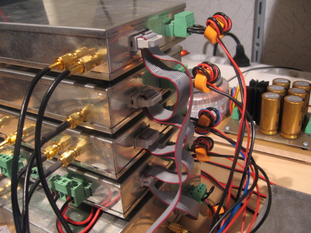
The common mode ferrite chokes in the output cabling further suppress these switcher spikes. The filtering as close as possible to the modules is depicted in the following photo, showing the power and I2C side of the experimental receiver signal path stack. (The Variable Gain Board is not yet there in this picture.) Four common mode turns are applied to the fairly large orange toroids. These are ferrites of unknown origin and material, which were available at a local shop for a very low price. The permeability of the orange cores is quite high: 4 turns give 60μH. Inner diameter is 8mm, outer diameter is 16mm and height is 8mm. Given those dimensions and inductance with 4 turns, the permeability is calutated to be 3516 so it can be positioned somewhere in between the 73 (μ=2500) and the 75 (μ=5000) material from Fair-Rite.
A large ferrite toroid is also used to choke the output cabling close to the Switcher Board. A toroid that can be opened and closed to make clamping around the entire bundle of wires easy is best used. This toroid has been scavenged from a broken computer monitor.
The extensive set of preventive measures to suppress switcher spurs is very effective. Only a few Switcher Board induced spurs in total can be found and the strongest ones are just below MDS level. If one is encountered in practice which is only possible with very little band noise coming from the antenna it can still be eliminated by toggling the switcher between 192KHz and 196KHz.
Assembly
The Switcher Board, fully assembled in its tin metal box, is depicted in the photo below.
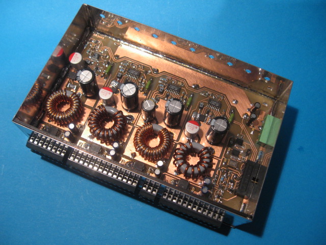
Note the ventilation holes at both sides of the board in the top and bottom side on the following photo. The box is meant to be mounted standing up with the output terminal blocks facing downwards. In that case these holes allow for a constant upwards convection at the component side and the ground-plane side, removing any need for active cooling. Actually the holes in the box are not really needed if only the receiver is being powered.
The bottom row of terminal blocks are all ground connections. The top row are the -14V, +14V, +18V and +5V supply outputs from left to right.
The module is euro-card sized and follows the general layout rules used consistently in this project:
-
Input power and special control connector are located at standard positions at the right edge of the board.
-
Output power terminal blocks are located at the bottom edge of the board.
Adjustment
No on-board "analog" adjustments are needed to commission the Switcher Board.
Solder jumper SJ1 is used to connect the INT and KILL lines in case no handshaking from an external MCU is needed when powering down.
Documentation
The following links point to the Switcher Board and Rectifier Board documentation files available for download for those who wish to reproduce the unit:
Switcher Board documentation in PDF format
Rectifier Board documentation in PDF format
This PDF's contains:
-
Schematics.
-
Bill of materials.
-
Component side, scale 1.3.
-
Back side, scale 1.3, showing the tracks to be wired by hand.
-
Top side, mirrored scale 1.0, for PCB production.
-
Bottom side, mirrored scale 1.0, for PCB production if needed.
Specification
The following table summarizes the key parameters of the Switcher Board:
| Switcher Board Specs |
| Dimensions |
160 x 100 x 50 |
mm |
| Weight |
650 |
gr. |
| Input Voltage |
+21 to +32 |
V |
| Under voltage protection shutdown voltage |
21.0 |
V |
| Under voltage protection hysteresis |
0.7 |
V |
| Over Voltage Protection (TVS diode) |
33.3 - 36.8 |
V |
| Output power at full load |
122 |
W |
| Efficiency at full load |
96 |
% |
| Switcher Clock Frequency |
192 or 196 |
KHz |
| +5V |
| Maximum output current |
4 |
A |
| Short circuit output current |
2.5 |
A |
| Over Voltage Protection (TVS diode) |
6 - ? |
V |
| Maximum output power |
20 |
W |
| Output voltage no load |
5.01 |
V |
| Output voltage full load (4A) |
4.94 |
V |
| Efficiency full load (4A) |
96 |
% |
| Terminal block connections |
12 |
# |
| +14V |
| Maximum output current |
4 |
A |
| Short circuit output current |
2.0 |
A |
| Over Voltage Protection (TVS diode) |
15.6 - 17.2 |
V |
| Maximum output power |
56 |
W |
| Output voltage no load |
14.94 |
V |
| Output voltage full load (4A) |
13.83 |
V |
| Efficiency full load (4A) |
98 |
% |
| Terminal block connections |
14 |
# |
| +18V |
| Maximum output current |
1 |
A |
| Short circuit output current |
0.46 |
A |
| Over Voltage Protection (TVS diode) |
20.0 - 22.1 |
V |
| Maximum output power |
18 |
W |
| Output voltage no load |
17.73 |
V |
| Output voltage full load (1A) |
17.42 |
V |
| Efficiency full load (1A) |
98 |
% |
| Terminal block connections |
3 |
# |
| -14V |
| Maximum output current |
2 |
A |
| Short circuit output current |
4 |
A |
| Over Voltage Protection (TVS diode) |
15.6 - 17.2 |
V |
| Maximum output power |
28 |
W |
| Output voltage no load |
-13.91 |
V |
| Output voltage full load (1A) |
-13.87 |
V |
| Efficiency full load (4A) |
91 |
% |
| Terminal block connections |
8 |
# |
The following table summarizes the key parameters of the Rectifier Board:
| Rectifier Board Specs |
| Dimensions |
300 x 115 x 70 |
mm |
| Weight |
3.1 |
Kg |
| Nominal Input Voltage |
115 or 230 |
Vac |
| Maximum sustained output power |
184 |
W |
| Output Voltage full load (184W) |
+24.5 |
V |
| Ripple voltage full load (184W) |
0.84 |
Vtt |
| Output Voltage half load (100W) |
+27 |
V |
| Ripple voltage half load (100W) |
0.45 |
Vtt |
| Output Voltage no load |
+30 |
V |
Conclusion
Using switched-mode power supplies in the context of a sensitive HF receiver comes with the challenge to almost completely suppress the interference caused by the switching. It turns out to be quite possible to contain the high frequency switching energy sufficiently inside the switcher box. Preventing ground loops, separation of power ground and signal ground, extensive additional filtering and common mode ferrite chokes are key factors in getting this result.
With the switching interference contained with only a few spurs on the lower HF-bands close to receivers noise floor, the main reward for the pre-regulator effort is very good efficiency. The secondary onboard LDO regulators in the various subsystems now only dissipate the minimum needed keeping the receiver stack much cooler. Also the fold back current characteristic of the positive power supplies improves safety. Furthermore the single unregulated power supply requirement of between +21V and +32V allows for powering by (car) battery by using two in series or by just one with an additional efficient booster switcher.
One other thing is worth mentioning here. The switching pre-regulators are very helpful in almost completely eliminating any mains induced hum and its harmonics in the audio subsystems. The inevitable 100Hz or 120Hz ripple of the unregulated power supply is completely suppressed by these switchers. This is visible in the spectrum analyzer shot shown for the Audio Board! There is a remote possibility, when the big toroidal mains transformer is mounted without a magnetic shield inside the receiver cabinet that some hum still might be picked up directly by the shielded audio cables between the Detector Board and the Audio Board.
This concludes the description of the Switcher Board.
Back to Receiver Overview
Back to the TOC
|