Block Diagram
The board that follows the Variable Gain Board in the signal path is the Detector Board. This board is the final board of the IF subsystem. It translates the IF signal down to the baseband. The block diagram is shown in the picture below:
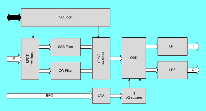
The -17dBm 9MHz IF signal enters the block diagram at the left where it first passes a noise filter before it is down converted by the product detector. The noise filter is selectable with I2C control. Either a 3-pole SSB filter or a 3-pole CW filter can be selected. The purpose of the noise filter is to block the wideband IF image noise seen by the product detector that would otherwise be mapped directly into the baseband, increasing the receivers cumulative noise figure unnecessarily.
The product detector is implemented with a Quadrature Sampling Detector or QSD. The QSD is also known as "Tayloe Detector" or should it actually be called the "Van Graas Detector"? Whoever invented the QSD first, it is often part of the hardware frontend in many popular SDR's today. It is chosen here for its very good linearity (IIP3 = +30dBm) which guarantees that no excess in-channel IMD will be added by the product detector. It also provides a quadrature (I-Q) output as a bonus. The IQ output is used as a binaural stereo output which provides more audio depth especially with CW and using a head-set. It can also be used to interface directly with a PC's soundcard for further digital signal processing on the PC.
One may wonder why the QSD has not been used as an image rejection mixer. This could have eliminated the complexity of the two crystal noise filters or not? The reason is that in that case the complexity would not have been reduced much! First of all an additional wide band phase shifting network is needed to obtain the image rejection in conjunction with the QSD and second, the noise filters are still needed in the audio path to block the down converted in-channel wideband noise contributed by the IF. In fact the noise filters are quite easy to implement at 9MHz with the QT quartz!
A divide by 4 IQ squarer is used to drive the QSD. This requires the BFO to operate around 4 times the IF frequency: 36MHz. A positive side effect of this choice is that it eliminates the possibility of direct BFO signal leakage into the very sensitive input of the 9MHz IF. The IQ squarer is a digital circuit that gives very precise IQ drive at 9MHz. In order to provide a fairly wide range of allowable BFO input signal a simple pre-amplifier has been added. The board can be driven directly with the filtered output of the DAC of a DDS chip.
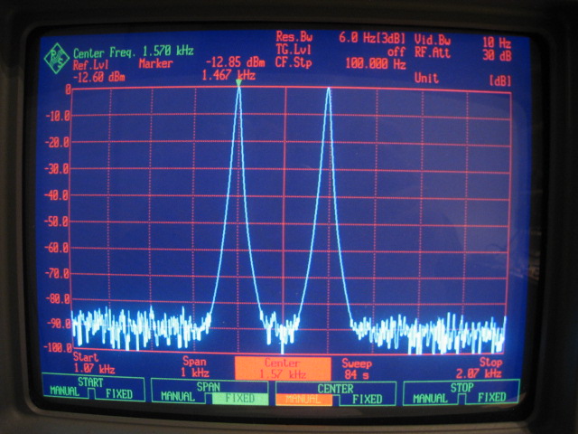
The following picture shows the relative absence of IMD observed at the output of the Detector Board. The 2-tone spacing is 200Hz. The combined 2-tone level at the input is -17dBm, which equals the nominal output level of the Variable Gain Board. The SSB noise filter is selected.
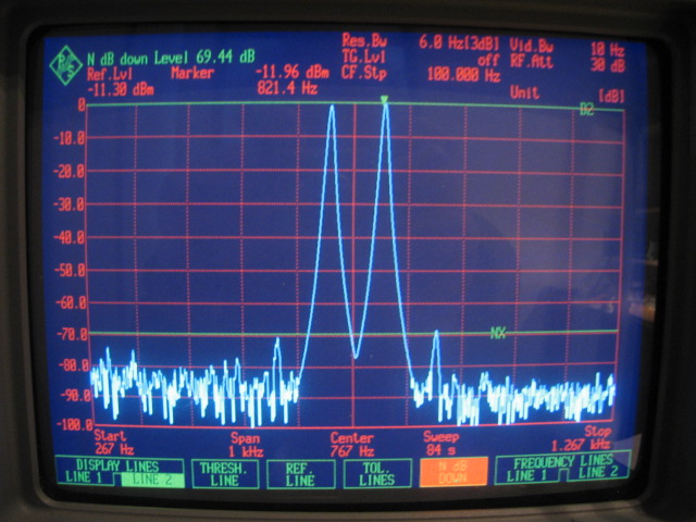
The next picture shows the IMD with 100Hz spacing, but now with the CW noise filter selected. IMD3 is now quite visible above the 6Hz noise floor, but still well below the -60dBc level of the Variable Gain Board!
Assembly
The Detector Board, fully assembled in its tin metal box, is depicted in the photo below.
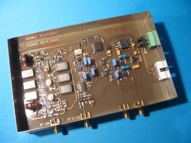
The module is euro-card sized and follows the general layout rules used consistently in this project:
-
Power and I2C control connector are located at standard positions at the right edge of the board.
-
SMA connectors are located at the bottom edge of the board and provide the signal interface to the board.
The board contains the following sub-circuits, which can be recognized from the picture:
-
Selectable 2400Hz and 500Hz 3-pole crystal noise filters.
-
Double balanced QSD.
-
BFO pre-amp and divide by 4 squarer.
-
A pair of simple low-pass audio filters.
-
I2C hardware to control the board through I2C with a microcontroller.
-
On-board LDO regulators and extra power supply filtering.
Adjustment
The only "analog" adjustment needed to commission the Detector Board is to center the CW noise filter exactly at 9MHz. Like with the CW roofing filter on the Frontend Board, this is best done with a VNA.
Solder jumpers SJ1, SJ2 and SJ3 determine the I2C address of IC14. They should be configured such that there are no conflicts on the I2C bus with the addresses of other I2C chips.
Solder jumpers SJ4 and SJ5, which enable I2C-bus terminating resistors R10 and R11 should only be soldered in if the Detector Board is positioned at the end of the physical I2C-bus.
Documentation
The following link points to the Variable Gain Board documentation file available for download for those who wish to reproduce the unit:
Detector Board documentation in PDF format
This PDF contains:
-
Schematics.
-
Bill of materials.
-
Component side, scale 1.6.
-
Back side, scale 1.6, showing the tracks to be wired by hand.
-
Top side, mirrored scale 1.0, for PCB production.
-
Bottom side, mirrored scale 1.0, for PCB production if needed.
Specification
The following table summarizes the key parameters of the Detector Board:
| Detector Board Specs |
| Dimensions |
160 x 100 x 30 |
mm |
| Weight |
290 |
gr. |
| Positive Supply Voltage |
+13.5 to +15 |
V |
| Positive Supply Current |
52 |
mA |
| Negative Supply Voltage |
-13.5 to -15 |
V |
| Negative Supply Current |
12 |
mA |
| Input Impedance |
50 |
Ω |
| Detector voltage gain |
11 |
dB |
| Noise filter center frequency |
9.000 |
MHz |
| -3dB bandwidth SSB noise filter |
2525 |
Hz |
| Insertion loss SSB noise filter |
-1.44 |
dB |
| IMD, -20dBm 2-tones with SSB noise filter |
< -90 |
dBc |
| -3dB bandwidth CW noise filter |
447 |
Hz |
| Insertion loss CW noise filter |
-3.26 |
dB |
| IMD, -20dBm 2-tones with CW noise filter |
-70 |
dBc |
| IQ amplitude balance |
0.1 |
dB |
| IQ phase balance |
< 1.0 |
° |
| Minimum BFO input level |
-15 |
dBm |
| Maximum BFO input level |
+12 |
dBm |
Please use the following links to navigate to the detailed discussions of the following subsystems:
Noise Filters
Quadrature Sampling Detector
Back to IF Introduction
Back to the TOC
|